
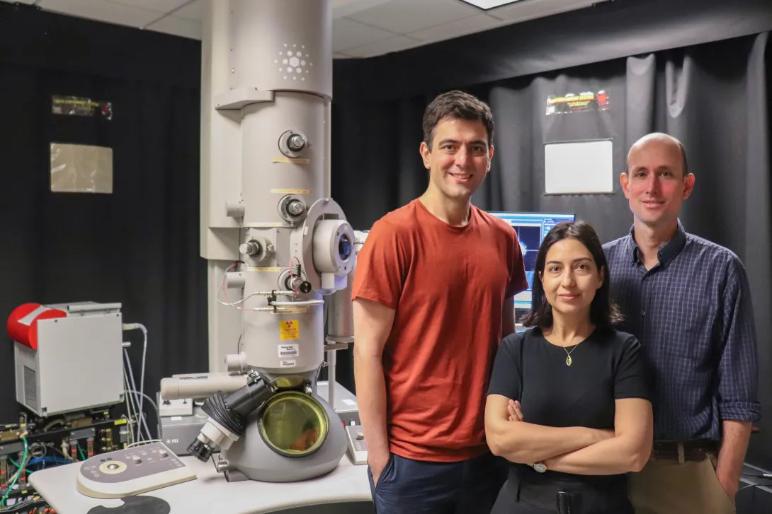
A photo of Vida Jamali, assistant professor the School of Chemical and Biomolecular Engineering; Amirali Aghazadeh, assistant professor in the School of Electrical and Computer Engineering; and Josh Kacher, associate professor in the School of Materials Science and Engineering standing in front of a TEM at Georgia Tech.
Scientific discovery is often portrayed as the result of long hours alone in a lab, but true science is inherently collaborative. The most robust experimental processes are developed through partnerships across multiple areas of research. The need for specialized, multidisciplinary teams slows experiment design, execution, data analysis, and process updates, delaying technological validation and deployment. But if the increasingly automated tools scientists already use in the lab could contribute to this team process of experimental design, the timeline for these goals could be greatly accelerated.
This concept of “lab tool as lab assistant” is the premise of a recent paper in npj | Computational Materials titled “Thinking Microscopes: Agentic AI and the Future of Electron Microscopy,” by Vida Jamali, assistant professor the School of Chemical and Biomolecular Engineering; Amirali Aghazadeh, assistant professor in the School of Electrical and Computer Engineering; and Josh Kacher, associate professor in the School of Materials Science and Engineering.
In the paper, the team introduces the concept of “thinking electron microscopes,” in which agentic AI systems are directly integrated with the instrument. This allows microscopes to move beyond their conventional role as characterization tools and toward functioning as co-scientists for human users.
Drawing on advances in specialized large language models, or LLMs, that demonstrate their ability to collaborate, reason over data, and integrate prior knowledge, the team envisions specialized LLM-based agents assigned to specific roles and areas of knowledge expertise. By explicitly incorporating domain knowledge into specialized agents and distributing information across multiple agents with focused expertise, the approach enables parallel evaluation of competing hypotheses, clearer separation of roles — such as planning, simulation, and critique — and more transparent and robust reasoning.
Within the experimental pipeline, these agents can analyze materials’ properties, physical data, chemical processes, and other relevant parameters. They could also collaborate with an agent that specializes in experimental design, refining iterative closed-loop experimentation, and real-time scientific discovery.
Although the research focuses on AI collaboration, the team notes that human researchers must retain accountability for the accuracy and integrity of both the experimental process and the results reported. This oversight begins with advocating for greater open access to research materials in all formats, building community-driven data repositories, and adopting standardization in how experimental parameters and metadata are reported. Equally important, researchers should be willing to report data from failed experiments as well as successful outcomes. Finally, organizations should work together to standardize secure APIs that enable shared, remote access to infrastructure across distances.
We see this as a step toward scientific instruments that do more than acquire data; systems that can reason over experiments, adapt measurements, and participate in the scientific discovery process alongside researchers. - Vida Jamali, assistant professor the School of Chemical and Biomolecular Engineering
The team is already developing these systems by connecting cloud-based, agentic infrastructures to microscopes at the Institute for Matter and Systems at Georgia Tech. With the addition of agentic AI, the goal is to accelerate discovery and engineering of new nanoscale materials for energy and quantum applications, as well as advance capabilities in cryo-electron microscopy and structural biology. These tools can optimize data collection, link real-time microscope observations with structural models of proteins, and dynamically adjust and prioritize experiments. The team sees this work as the first step toward the next generation of “thinking” electron microscopes, as well as an advancement in scientific discovery across domains.
- Christa M. Ernst
This research is supported by the Institute for Data Engineering and Science and the Institute for Matter and Systems
Original Publication
Jamali, V., Aghazadeh, A. & Kacher, J. Thinking microscopes: agentic AI and the future of electron microscopy. npj Computational Materials 12, 149 (2026). https://doi.org/10.1038/s41524-026-02077-y
News Contact
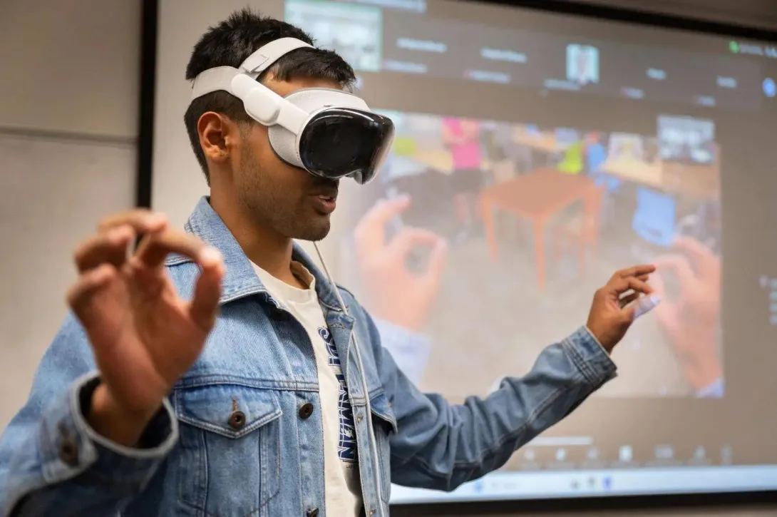
Georgia Tech student Yash Rajgure using an Apple Vision Pro headset device to demo his team's project in ECE 6001 Technology Entrepreneurship: Teaming, Ideation, and Entrepreneurship. Photo: Allison Carter, Georgia Tech
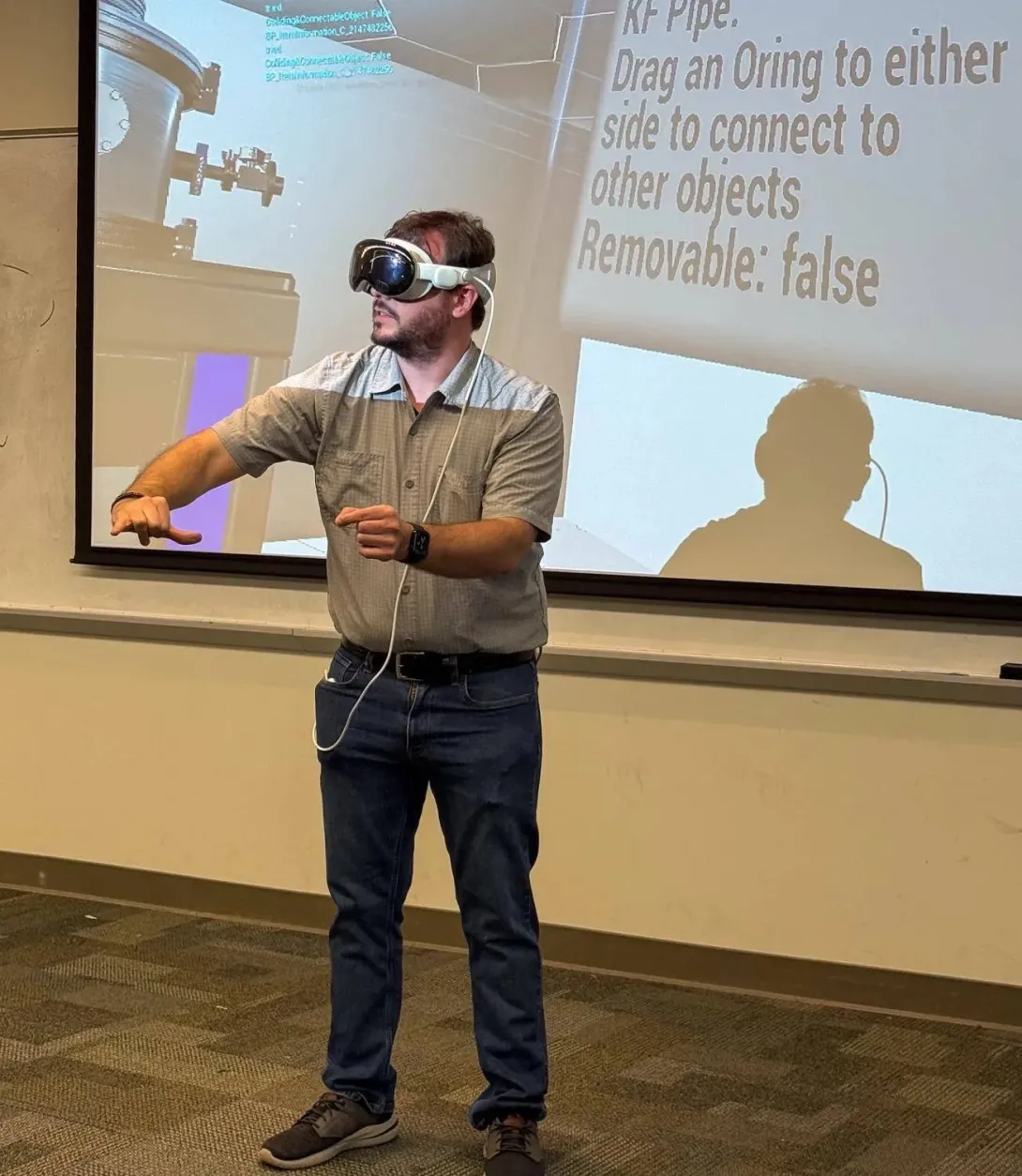
Gallmon showing how Apple Vision Pro can be utilized to train students and workers on sensitive and expensive technical equipment, in this case a cleanroom vacuum system.
Learning electrical and computer engineering has always come with a unique challenge: many of its foundational concepts — electric fields, magnetic forces, semiconductor behavior — are invisible to the naked eye and difficult to visualize.
To make these invisible principles tangible, students in the School of Electrical and Computer Engineering have long used specialized tools and software. Circuit simulators model voltage and current, electromagnetic tools visualize fields, and semiconductor design platforms reveal transistor behavior. These tools turn abstract theory into interactive experiences that prepare students for real-world engineering challenges.
Now, Apple Vision Pro is joining this ecosystem.
The technology introduces spatial computing to learning environments, blending digital content with the physical world.
At the Institute for Matter and Systems, infrastructure lead Alex Gallmon, is collaborating with students and industry partners to create immersive digital twins—virtual models that replicate real-world systems—of semiconductor cleanroom equipment.
“These machines are complex and costly, with parts that can run tens of thousands of dollars,” he said. “Even minor mistakes during operation can lead to expensive damage or downtime.”
Gallmon's team built a virtual replica of a cleanroom vacuum training system. The project serves as a prototype for a workforce development program aimed at high school and college students interested in careers in the semiconductor or vacuum technology fields.
Read the full story from the School of Electrical and Computer Engineering
News Contact
Dan Watson | School of Electrical and Computer Engineering

The National Academy of Inventors is honoring two Georgia Tech faculty members for their contributions to technology and society: Deepakraj “Deepak” Divan and Arijit Raychowdhury. Both are in the School of Electrical and Computer Engineering.
Raychowdhury is a semiconductor pioneer whose patented circuit and system-on-chip designs have advanced computing efficiency and commercialization. Divan is a global leader in power electronics and grid modernization, whose innovations and ventures have transformed how electricity is delivered and managed worldwide.
“Congratulations to Deepakraj and Arijit on earning one of the most esteemed accolades in technology and discovery. Their groundbreaking work, with nearly 100 patents between them, advances solutions to global challenges,” said Raghupathy “Siva” Sivakumar, chief commercialization officer at Georgia Tech. “Their success exemplifies how research commercialization drives real-world impact, and we’re proud to see them honored as academy fellows.”
Election to NAI is the highest professional distinction specifically awarded to inventors. With this recognition, Georgia Tech’s roster of NAI Fellows grows to 24. Divan and Raychowdhury join a 2025 class of 169 new fellows representing university, government, and nonprofit organizations worldwide. They will be inducted at the NAI 15th Annual Conference on June 4, 2026, in Los Angeles.
Deepakraj “Deepak” Divan
Professor Emeritus (2004-2025)
Georgia Research Alliance Eminent Scholar
School of Electrical and Computer Engineering
Founder, Georgia Tech Center for Distributed Energy
Deepakraj “Deepak” Divan is a globally recognized innovator in power electronics and grid transformation. He was awarded the IEEE Medal in Power Engineering in 2024.
He holds over 85 U.S. and international patents and has authored 400 refereed publications. His pioneering work on soft‑switching converters—integral for efficient energy storage, EV charging, and industrial controls—has spurred a global $70 billion power electronics industry.
Divan laid the groundwork for grid‑forming inverter control, enabling high-renewables integration. He is the co-author of Energy 2040: Aligning Innovation, Economics and Decarbonization, named by Forbes as one of the “10 Essential Books and Podcasts Every Leader Needs in 2025”.
“Being named an NAI Fellow is a tremendous honor,” said Divan. “It reflects years of effort to rethink how electricity is delivered and managed to solve real problems and to drive practical innovations that matter.”
As the founder of Georgia Tech’s Center for Distributed Energy, he led research that transforms electricity delivery through analytics, monitoring, and optimization.
An entrepreneur, Divan co-founded Varentec (backed by Bill Gates and Khosla Ventures) and seeded ventures including GridBlock, Soft Switching Technologies, Innovolt, and Smart Wires—raising over $500 million. A National Academy of Engineering member and IEEE Fellow, he champions scalable energy-access solutions worldwide.
Arijit Raychowdhury
Professor and Steve W. Chaddick School Chair
School of Electrical and Computer Engineering
Director, Center for the Co-Design of Cognitive Systems
Arijit Raychowdhury has been the Steve W. Chaddick School Chair of ECE since 2021. He is a leading innovator in semiconductor technologies, holding more than 27 U.S. and international patents and authoring over 350 publications.
His work spans low-power circuits, specialized accelerators, and system-on-chip design, with breakthroughs widely adopted in industry.
“This recognition reflects the collective effort of students, colleagues, and partners who share a vision for advancing microelectronics,” said Raychowdhury. “I am honored that NAI champions the same mission to lead through research, education, and innovation."
At Texas Instruments, he developed the world’s first adaptive echo-cancellation network for integrated Digital Subscriber Lines (DSL)—a patented technology that enabled high-speed internet over traditional phone lines that received the EDN Innovation of the Year award. At Intel, he developed and incorporated foundational memory and logic technologies that shaped commercial products across global markets for more than a decade.
His research on fine-grain power management of systems-on-chip at Georgia Tech has been licensed and widely adopted by the semiconductor industry.
He directs Georgia Tech’s Center for the Co-Design of Cognitive Systems and leads initiatives to advance microelectronics design with applications to AI. Over the years, he has served as a founding advisor and board member to multiple startups in the areas of edge-computing and low power design.
Raychowdhury’s research bridges invention and real-world impact, earning him numerous honors, including IEEE Fellow, Semiconductor Research Corporation Technical Excellence Award, and multiple industry awards. Through pioneering designs and mentorship, he continues to drive innovation in computing systems, influencing both academic research and industrial commercialization.
News Contact
Dan Watson
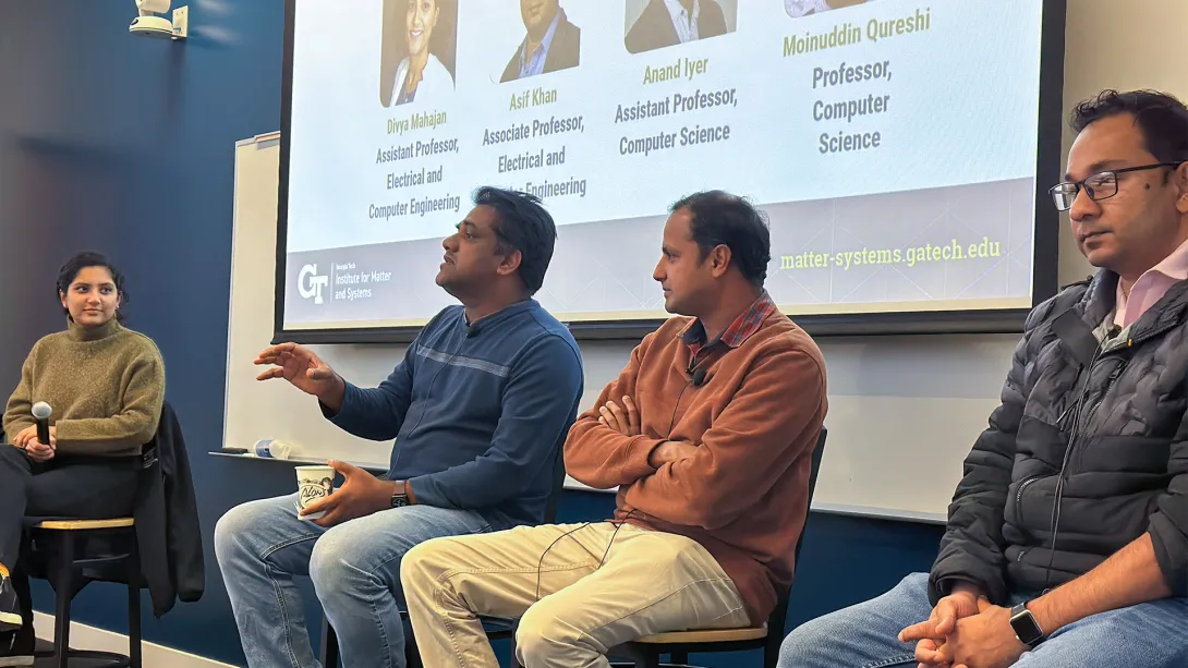
The Institute for Matter and Systems (IMS) hosted the inaugural Boundaries and Breakthroughs panel on Nov. 11, setting the stage for a new era of interdisciplinary dialogue at Georgia Tech. The event, held in the Marcus Nanotechnology building, brought together experts in electrical engineering, computer architecture, and computer systems design to tackle one of today’s pressing challenges: artificial intelligence (AI) scalability and sustainable high-performance computing.
As one of Georgia Tech’s 11 interdisciplinary research institutes, IMS is designed to break down silos between traditional academic units. By operating core user facilities and fostering collaborative research, IMS creates a unique ecosystem where device-level innovation meets systems-level design. This event personified that mission by connecting researchers who typically work on different ends of the stack.
“We’re looking for opportunities to bring people together to have discussions that are both informative and potentially create a little bit of friction in the best possible way around trending topics in science and engineering,” said Mike Filler, IMS deputy director, during opening remarks.
The panel was moderated by Divya Mahajan, assistant professor in the School of Electrical and Computer Engineering, and featured Moinuddin Qureshi, professor of computer science; Anand Iyer, assistant professor of computer science; and Asif Khan, associate professor in electrical and computer engineering.
The discussion explored the dynamics between compute abundance and energy constraints. As AI models scale up, power consumption has become a societal issue, driving up energy demands and even influencing political conversations. The panelists agreed that the bottleneck isn’t compute — a computer’s ability to process and execute tasks — but data movement. Moving data uses 100 to 1,000 times more energy than computation, making memory systems the critical frontier.
The conversation highlighted how breakthroughs in compute must occur at every layer — from individual devices to full computer systems. At the device level, Khan mentioned emerging memory technologies and “beyond CMOS” approaches such as embedding compute within memory and exploring bio-inspired architectures.
From a computer architecture level, Qureshi advocated rethinking interfaces and creating designs optimized for the future of computing. AI needs regular patterns to work optimally, and current patterns are not set up for that.
“If you want efficiency, design systems that make sense for AI,” Qureshi said. “Develop new interfaces, develop new modules, architectures, and organization that make for a specific pattern.”
At the systems level, Iyer stressed practical strategies like near-memory compute and energy-aware scheduling while acknowledging the need for co-design between hardware and software.
“Now in terms of brains or bio-inspired computing, my conjecture is that there is currently no hardware that is capable of doing it,” Khan said. He also noted that right now, there is no computer or algorithm that has the scale of computing comparable to human brain power.
The panelists didn’t shy away from provocative ideas — such as whether graphic processing units are the final solution for AI and whether matrix multiplication alone can lead to artificial general intelligence. While opinions varied, all agreed that organizations like IMS are key to bringing together diverse expertise to tackle these questions collaboratively.
The Boundaries and Breakthroughs series continues in January with a panel on bioelectronics and medical technologies, reinforcing IMS’s commitment to fostering dialogue that spans the full spectrum of innovation.
News Contact
Amelia Neumeister | Research Communications Program Manager
The Institute for Matter and Systems
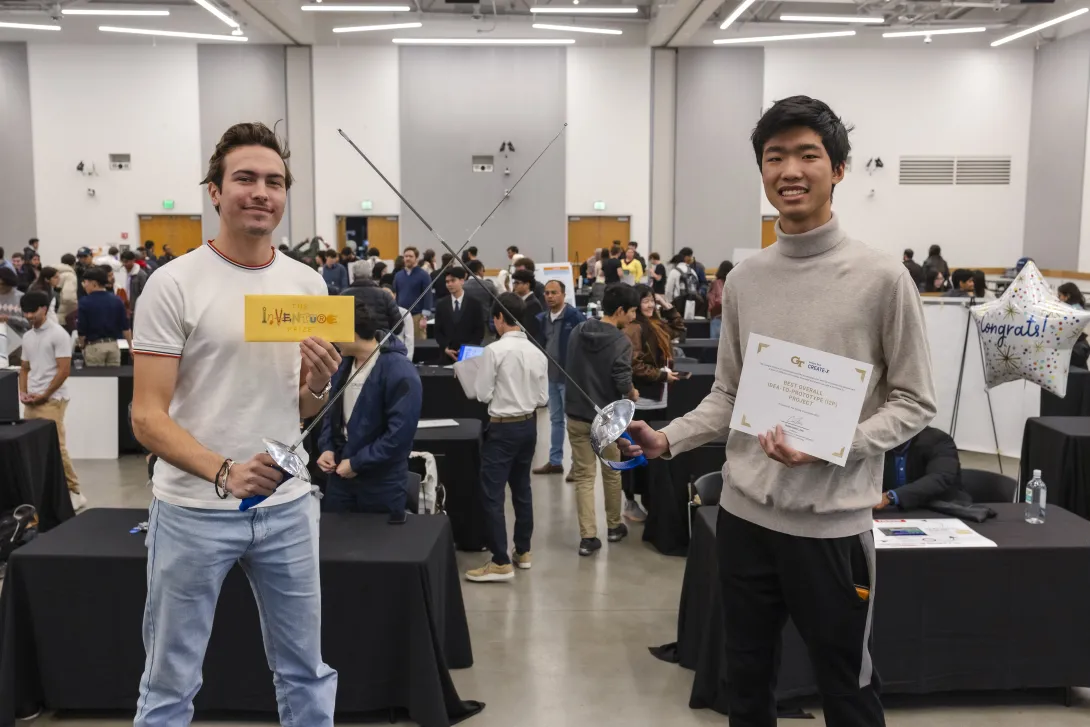
Founders of Allez Go: Adam Kulikowski and Jason Mo
Cricket powder-based protein brownies. A visualization system for fencing blades. A personalized AI application for analyzing blood work. All I2P Showcase prototypes. See what Georgia Tech students have been developing this semester at the Fall 2025 Idea to Prototype (I2P) Showcase on Tuesday, Dec. 2, at 5 p.m. in the Marcus Nanotechnology Building. This year, attendees will have even more original inventions to view, with over 60 teams displaying prototypes.
The event marks the culmination of the semester-long I2P course, where undergraduate students develop functional prototypes aimed at solving real-world problems. Prototypes this semester include a smart military drone, a gentler device for cervical cancer screening, a rotating espresso station, tools to keep AI safe, compact data centers, systems that simulate cyberattacks to help companies strengthen their defenses, and many more.
The showcase is free and open to students, faculty, staff, and members of the local community.
Winning teams will receive prizes and a “golden ticket” into CREATE-X’s Startup Launch, a summer accelerator that provides optional seed funding, accounting and legal service credits, mentorship, and more to help students turn their prototypes into viable startups.
This is a free event, and refreshments will be provided. Register for the Fall 2025 I2P Showcase today!
News Contact
Breanna Durham
Marketing Strategist
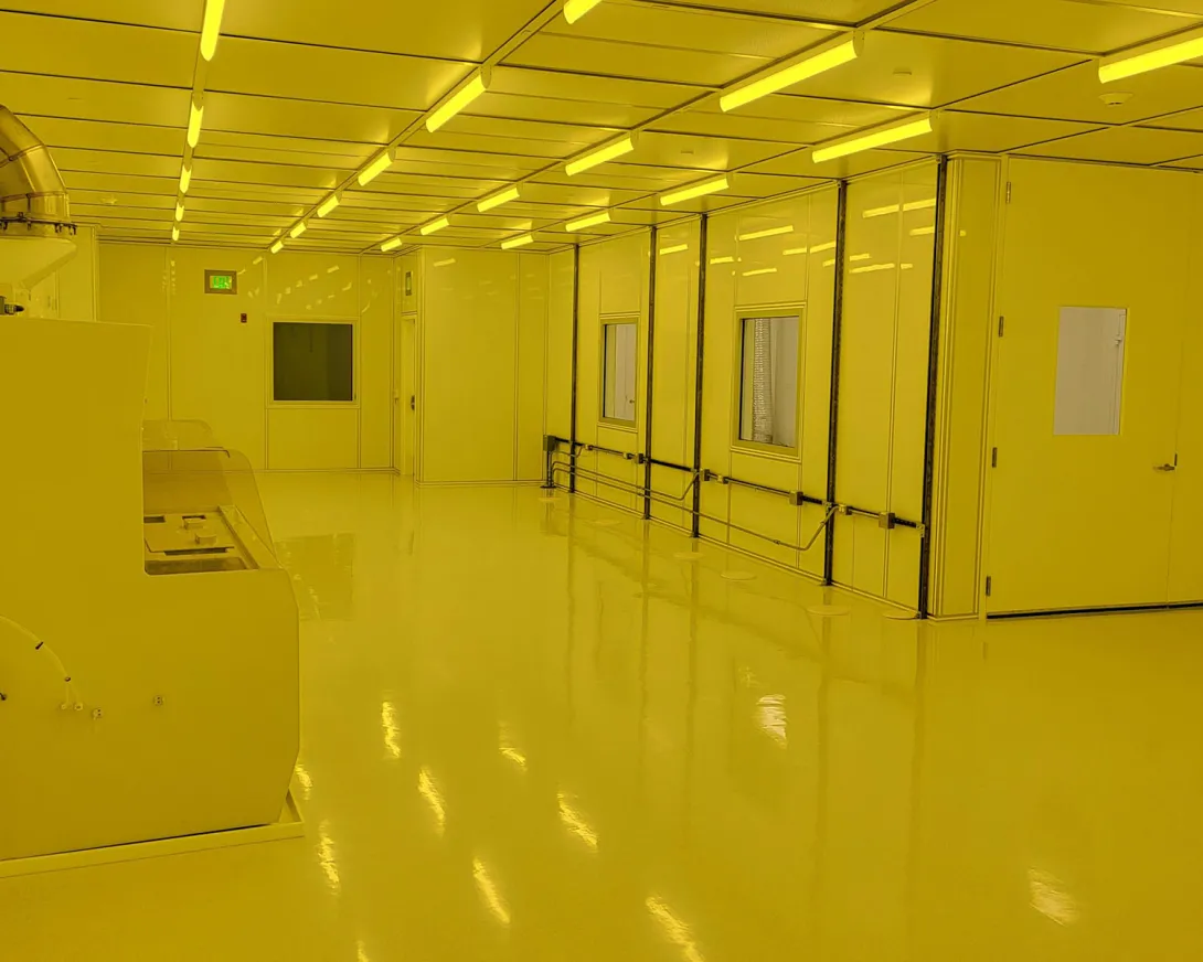
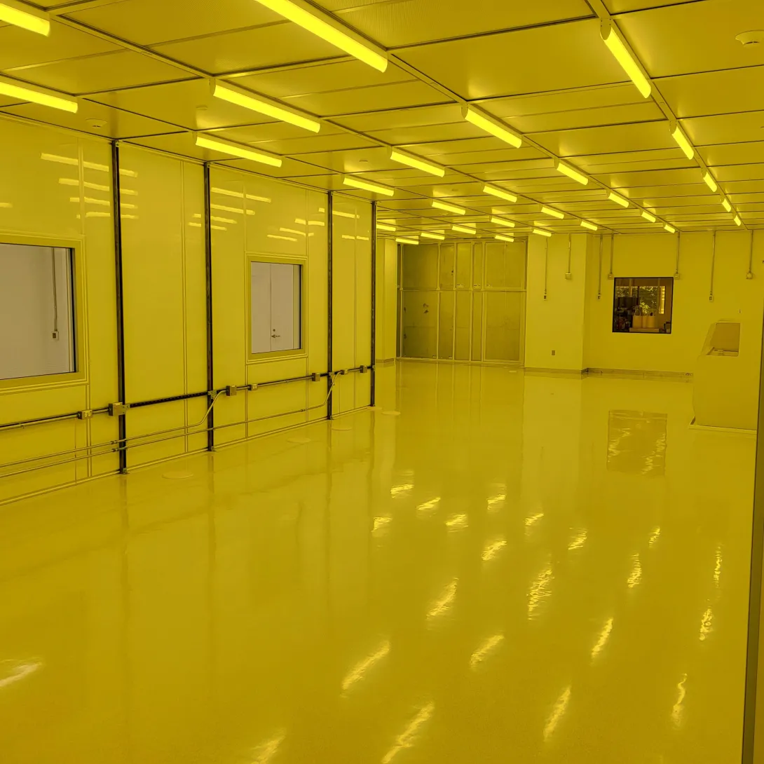
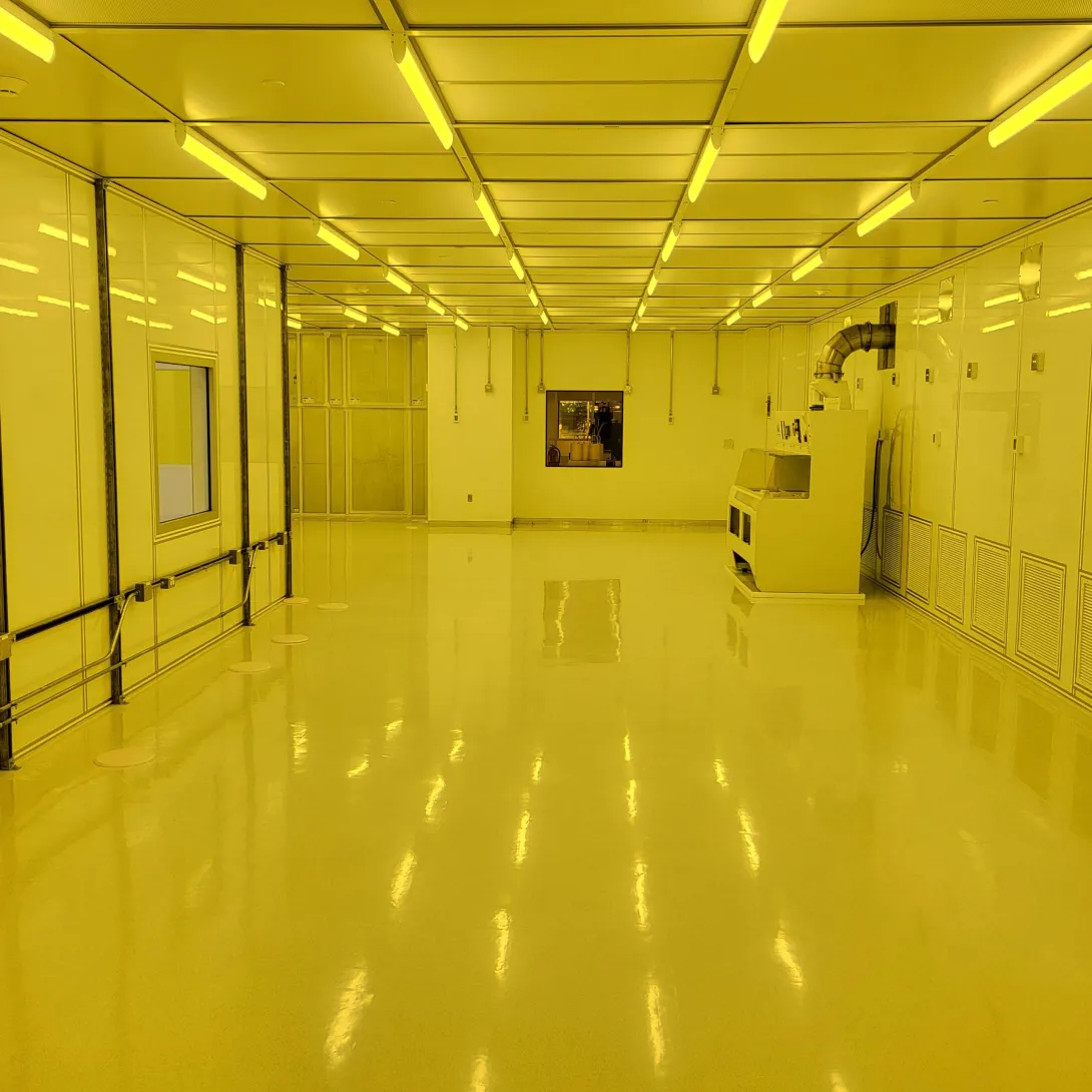
The Institute for Matter and Systems (IMS) has completed a major expansion of its cleanroom facilities, which now totals more than 23,000 square feet – solidifying its position as the largest academic cleanroom in the Southeast.
The expansion includes a newly constructed 2,000-square-foot ISO 6 cleanroom, designed to house an advanced packaging and 3D heterogeneous integration (3DHI) facility.
“As demand for cleanroom facilities continues to rise across academia and industry, this expansion strategically positions Georgia Tech to support national initiatives and advance global leadership in semiconductor packaging technologies,” said Gary Spinner, associate director of cleanroom and fabrication facilities at IMS.
This state-of-the-art space will be equipped with next-generation processing and inspection capabilities that represent the next generation of semiconductor manufacturing technology.
“The new facility, in conjunction with our existing Marcus facilities, will provide the campus community and our industry and government partners with the tools and capabilities to pursue revolutionary technologies in advanced packaging and 3D heterogeneous integration,” said Muhannad Bakir, Dan Fielder Professor in the School of Electrical and Computer Engineering and director of the 3D Systems Packaging Research Center (PRC). “These innovations will include developing radical advanced packaging and 3D stack architectures that seamlessly integrate electronics, photonics, power delivery, and thermal technologies.”
The PRC will use the new facility for advanced packaging research supported by multiple national programs and industry partnerships.
This robust infrastructure will support emerging applications in artificial intelligence, high-performance computing, and advanced mm-wave and photonic communications systems. By enabling the dense integration of multiple specialized chips within substrates and chip stacks, the pursued advanced packaging research will deliver more scalable, powerful and energy efficient systems at lower cost and shorter design cycles.
News Contact
Amelia Neumeister | Research Communications Program Manager
The Institute for Matter and Systems
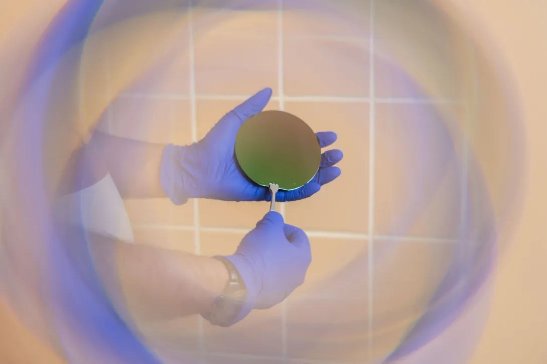
Silicon-on-insulator (SOI) wafer used in a multi-chip module featuring 3D optical interconnects. (Photo: Allison Carter)
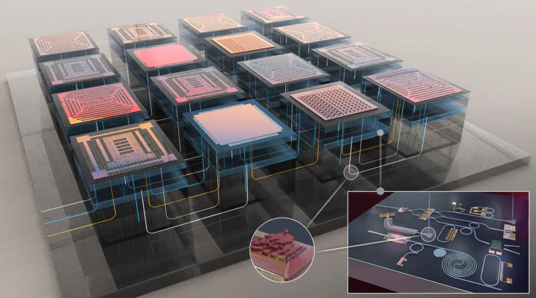
A schematic illustration of a multi-chip structure with 3D optical routing. The key parts of Adibi's proposed system are: 1) multi-layer planar waveguides, 2) free-form couplers, and 3) a dense vertical waveguide array.
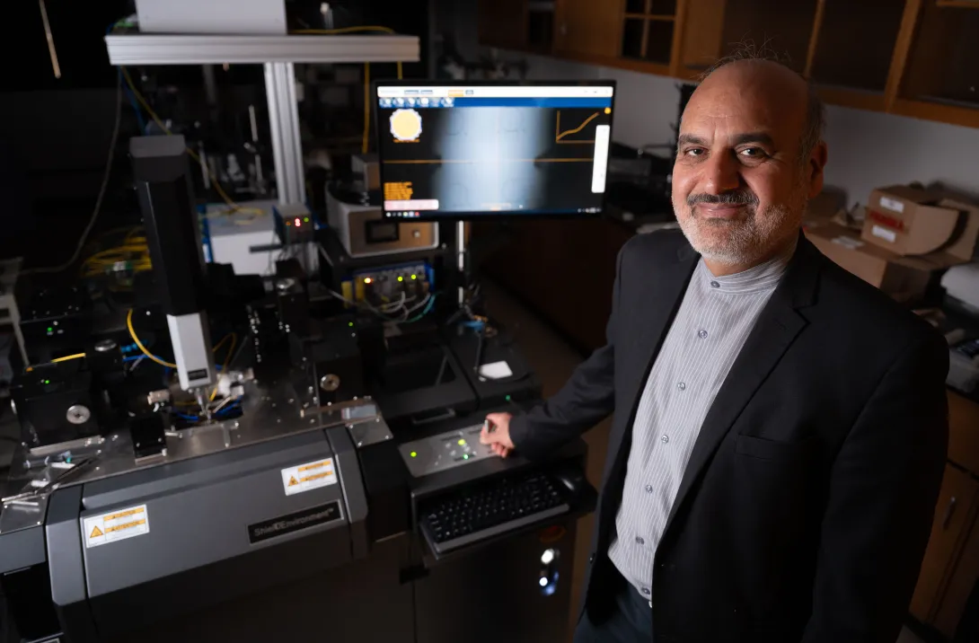
By combining advanced optical techniques, Professor Ali Adibi’s 3D optical routing systems looks to enable vertical chip integration in a way not previously achieved. (Photo: Allison Carter)
The future of computing is lit, literally.
As microchips grow more complex and data demands intensify, traditional electrical connections are hitting their limits. Speed is king in today’s digital systems, but a major bottleneck remains in how quickly information can move between components like processors and memory.
This lag is one of the most pressing challenges in advanced hardware design. While processors continue to accelerate, the links that connect them can't keep pace.
Georgia Tech researcher Ali Adibi is addressing this problem with $5.3 million in funding over three years from the Defense Advanced Research Projects Agency (DARPA). His project is part of DARPA’s Heterogeneous Adaptively Produced Photonic Interfaces (HAPPI) program, which aims to dramatically boost the speed and density of data transmission within microsystems by using light instead of electricity.
“Optical solutions are highly advantageous for providing the required data rates and power consumptions, and our project is formed to address the most important challenges for achieving the system-level performance,” said Adibi, a professor and Joseph M. Pettit Chair in the School of Electrical and Computer Engineering.
The project brings together a multidisciplinary team, including collaborators from the Massachusetts Institute of Technology, University of Florida, NY CREATES, and NHanced Semiconductors, Inc.
Going Vertical
Unlike traditional optical communication, which connects systems across distances, this project focuses on enabling ultra-fast, low-loss communication withinelectronic systems.
The key innovation is vertically connecting electronic chips in a compact stack. This design helps overcome the limitations of planar optical routing geometries (layouts that guide light horizontally across a chip) which are often not compatible with the dense, 3D chip architectures needed for next-generation computing.
Adibi’s team is developing a novel 3D optical routing system that can transmit data with minimal loss, high bandwidth, and compact components. The system is designed to scale to large arrays of interconnected chips with minimal interference between data channels.
Smarter Design with Machine Learning
At the heart of the project is the use of machine learning (ML) to help design and optimize the light-based communication system.
ML is used to shape and fine-tune the tiny structures that guide light through and between chips. This includes finding the best sizes, shapes, and layouts for components like couplers and waveguides, so they can be made smaller, work more efficiently, and fit into dense chip layouts.
“Designing a complete, scalable 3D optical routing structure involves innumerable variables,” Adibi said. “Machine learning helps us navigate that complexity and find solutions that would be nearly impossible to identify manually.”
Tiny "Mirrors"
Another key innovation involves specialized optical structures, or what Adibi refers to as “artificial mirrors”.
The tiny, precisely shaped structures, called metagratings, are embedded in the chip material to redirect light vertically between layers with minimal loss. These components are designed to guide light efficiently in tight spaces, helping connect stacked chips without losing signal strength.
“Imagine light traveling through a chip and suddenly being redirected straight up. That’s the kind of precise control we’re achieving,” Adibi explained.
These innovations, along with advanced techniques for building vertical light paths through thick silicon layers and new packaging solutions that keep components precisely aligned, have shown promise on their own. But combining them is what enables dense, high-speed, low-loss communication between vertically stacked chips, something that no system has achieved before, according to Adibi.
“As with any complex system, success depends on how well everything is structured and optimized,” he said. “Once everything is in alignment, data can move faster, more efficiently, and with less energy consumption for communicating each bit of data.”
About the Research
This research is supported by the Defense Advanced Research Projects Agency (DARPA) Heterogeneous Adaptively Produced Photonic Interfaces (HAPPI) program. Notice ID DARPA-SN-24-105.
News Contact
Dan Watson
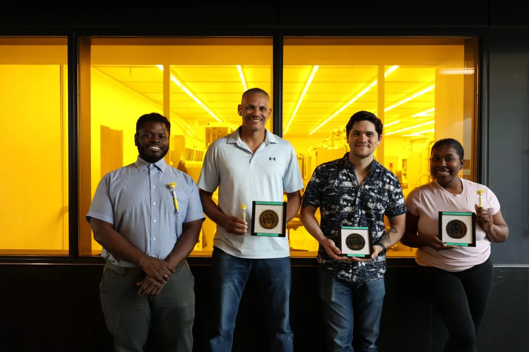
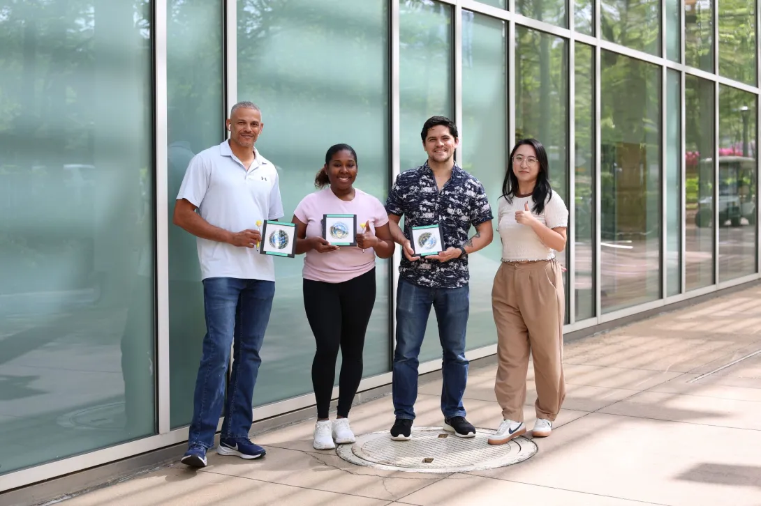
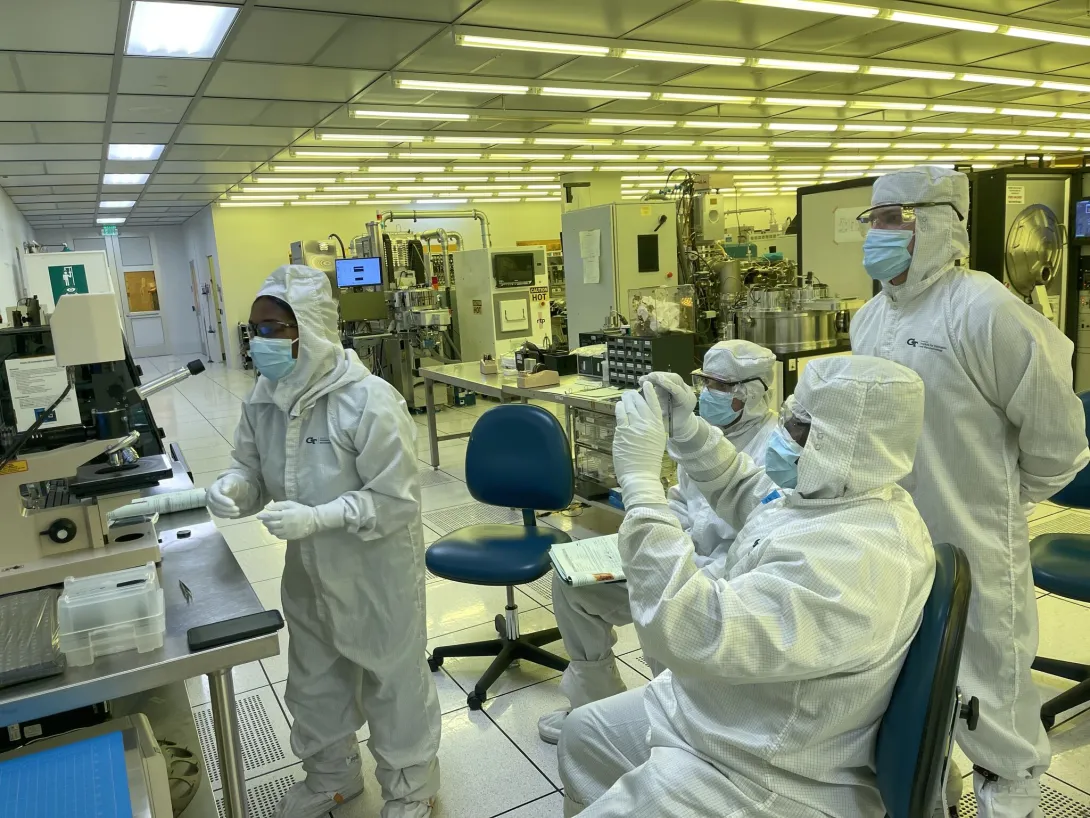
The most recent cohort of the Microelectronics and Nanomanufacturing Certificate Program (MNCP) have completed their training and are ready to dive into the workforce.
The MNCP is a National Science Foundation (NSF) funded collaboration between the Institute for Matter and Systems (IMS), Georgia Piedmont Technical College (GPTC) and Pennsylvania State University’s Center for Nanotechnology Education and Utilization.
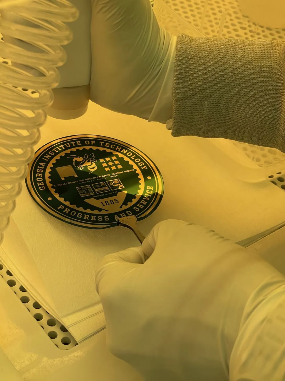
The spring 2025 cohort was comprised of three individuals with non-technical backgrounds. For 12 weeks, they split time between online lectures and hands-on training in the Georgia Tech Fabrication Cleanroom where they immersed themselves in advanced microelectronic fabrication techniques. Their training included thin film deposition, photolithography, etching, metrology, laser micro-machining, and additive manufacturing. They gained hands-on experience with industry-standard equipment, even creating their own custom designs on 4-inch silicon wafers.
“The program really helps people get their head start, especially for those who don’t really have the educational background,” said Lauren Walker, one student from the cohort. Walker applied for the program after hearing about it from a colleague and was able to get a job as a laboratory technician with help from the program resources.
“[The program] gave me everything I needed to know for new skills and things like that for the industry,” said Walker. “It helped me eventually get another job. I say it helped because of the workshops they had.”
Under the direction of Seung-Joon Paik, IMS teaching lab coordinator, the cohort spent two days a week in the IMS cleanroom working on research projects with IMS staff. Michelle Wu, a research scientist in IMS, served as lab instructor throughout the program and oversaw the training on cleanroom tools.
“As their lab instructor, I’ve been thoroughly impressed with their passion, patience, and unwavering dedication to this program,” said Wu.
The program is supported by the Advanced Technological Education program at the National Science Foundation and is free for all participants.
Learn more about the Microelectronics and Nanomanufacturing Certificate Program
News Contact
Amelia Neumeister | Research Communications Program Manager
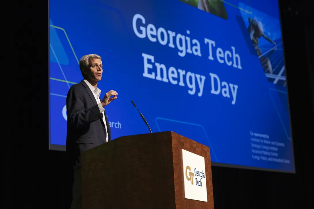
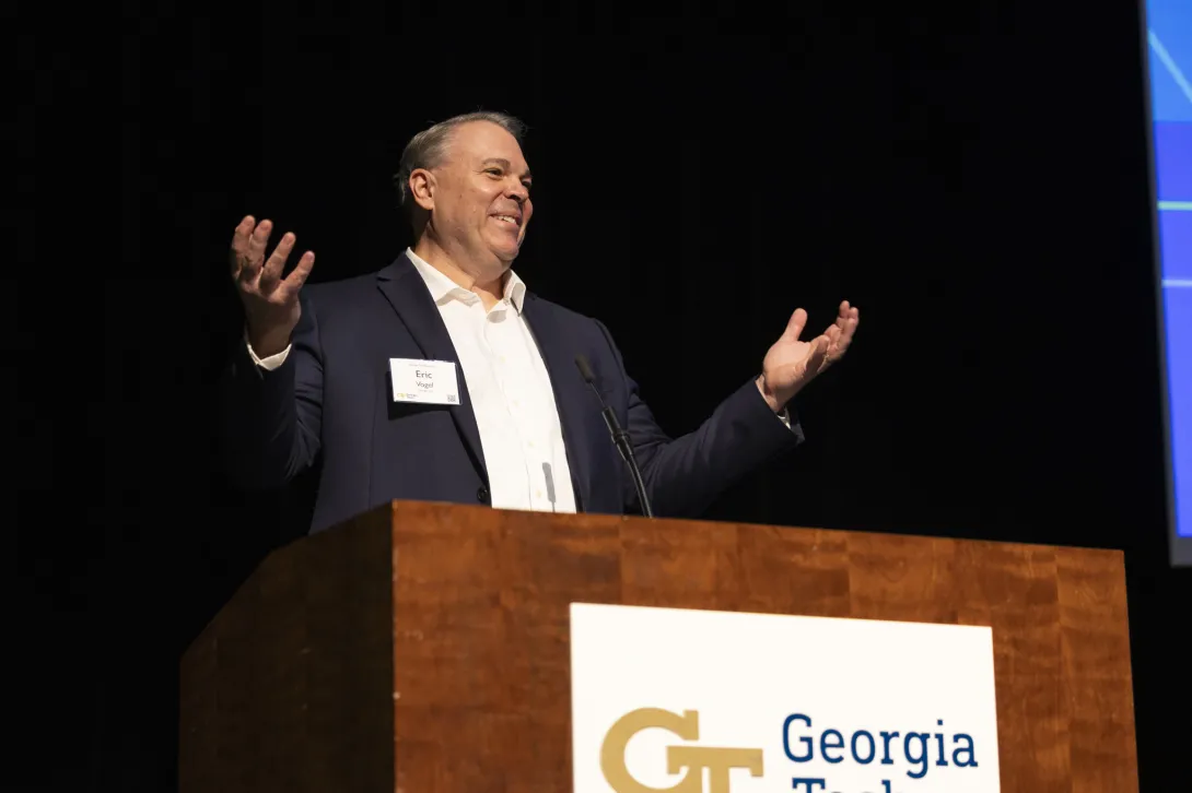
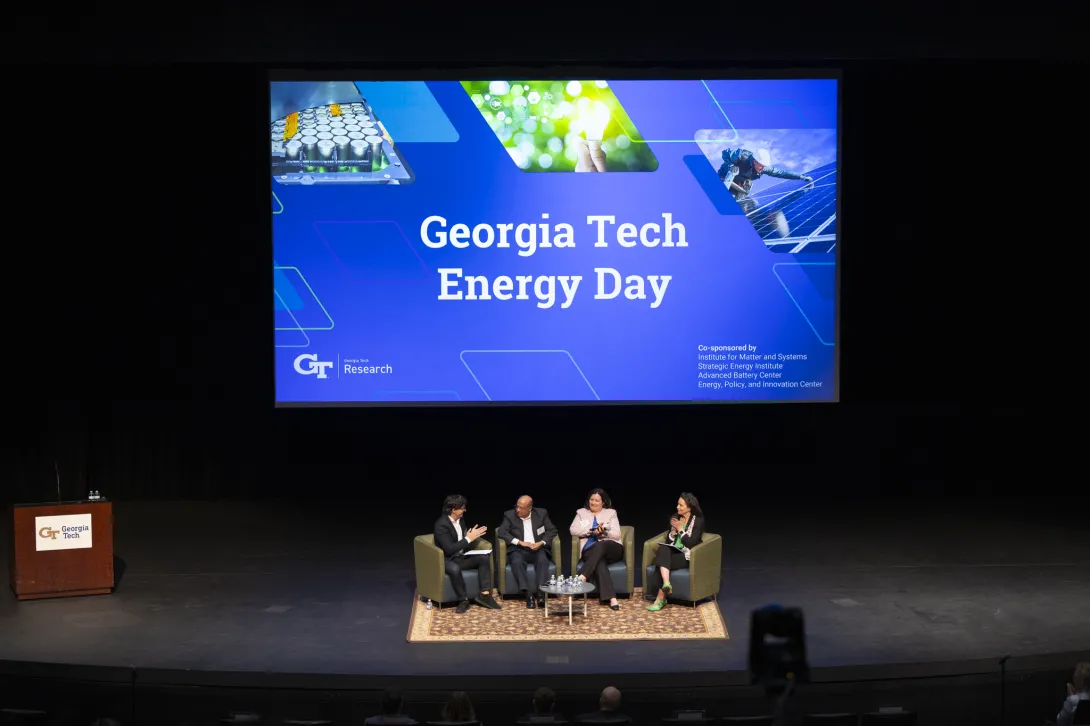
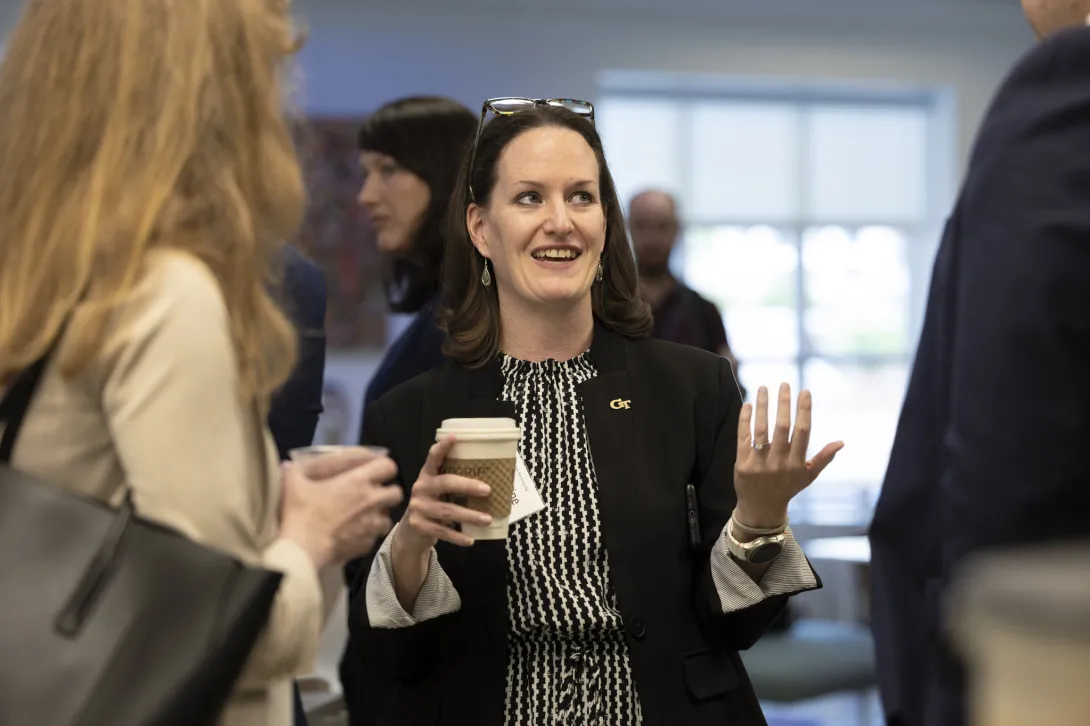
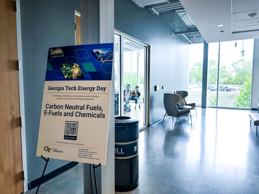
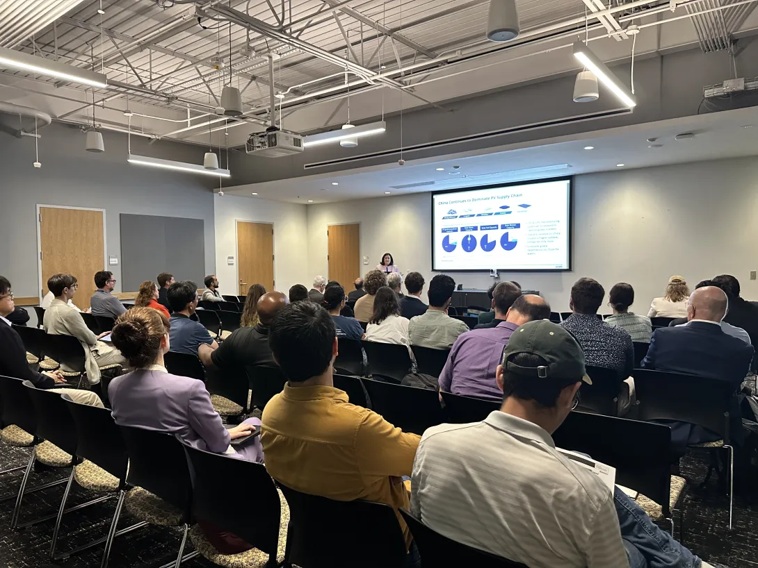
More than 300 people from industry, government, and academia converged on Georgia Tech’s campus for Energy Day. They gathered for discussion and collaboration on the topics of energy storage, solar energy conversion, and developments in carbon-neutral fuels.
Taking place on April 23, Energy Day was cohosted by Georgia Tech’s Institute for Matter and Systems (IMS), Strategic Energy Institute (SEI), the Georgia Tech Advanced Battery Center, and the Energy Policy and Innovation Center.
“The ideas coming out of Georgia Tech and other research universities can drive greater partnerships with our local and state officials. Whether you live in Georgia or elsewhere, we are changing how energy is viewed and consumed,” said Tim Lieuwen, Georgia Tech executive vice president for Research.
Energy Day 2025 is the latest evolution in a series of events that began as in 2023 Battery Day. As local and national energy research needs have evolved, the event has grown to highlight Georgia Tech, and the state of Georgia, as a go-to location for modern energy companies.
“At Georgia Tech, we approach energy holistically, leveraging innovative R&D, economic policy, community-building and strategic partnerships,” said Christine Conwell, SEI's interim executive director. “We are thrilled to convene this event for the third year. The keynote and sessions highlight our comprehensive strategy, showcasing cutting-edge advancements and collaborative efforts driving the next big energy innovations."
The day was divided into two parts: a morning session that included a keynote speaker and two panels, and an afternoon session with separate tracks addressing three different energy research areas. Speakers shared research being conducted at Georgia Tech, as well as updates from industry leaders, to create an open dialogue about current energy needs.
“We believe we can solve problems and build the economy when you bring various disciplines together and work from matter — the fundamental scientists and devices all the way out to final systems at large — economic systems, societal systems,” said Eric Vogel, executive director for IMS. “Not only did we share the latest research, but we discussed and debated how we can continue to transform the energy economy.”
Discussions ranged from adapting to rapid changes in battery storage to advancing photo-voltaic manufacturing in the U.S. to the environmental impacts and sustainable practices of e-fuels and renewable energy.
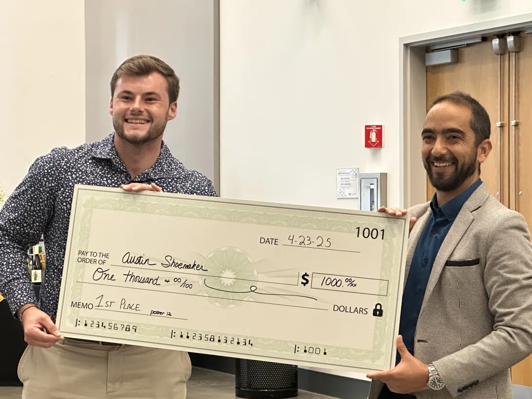
The day ended with a robust poster session that attracted more than 25 student posters presentations. Three were awarded best posters.
First place: Austin Shoemaker
Second Place: Roahan Zhang
Third Place: Connor Davel
Related Links:
Advancing Clean Energy: Georgia Tech Hosts Energy Materials Day
Georgia Tech Battery Day Reveals Opportunities in Energy Storage Research
News Contact
Amelia Neumeister | Research Communications Program Manager
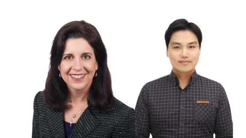
Michelle LaPlaca (left), associate chair for Faculty Development and professor in the Department of Biomedical Engineering; W. Hong Yeo, Harris Saunders, Jr. Professor in the George W. Woodruff School of Mechanical Engineering.
Georgia Tech professors Michelle LaPlaca and W. Hong Yeo have been selected as recipients of Peterson Professorships with the Children’s Healthcare of Atlanta Pediatric Technology Center (PTC) at Georgia Tech. The professorships, supported by the G.P. “Bud” Peterson and Valerie H. Peterson Faculty Endowment Fund, are meant to further energize the Georgia Tech and Children’s partnership by engaging and empowering researchers involved in pediatrics.
In a joint statement, PTC co-directors Wilbur Lam and Stanislav Emelianov said, “The appointment of Dr. LaPlaca and Dr. Yeo as Peterson Professors exemplifies the vision of Bud and Valerie Peterson — advancing innovation and collaboration through the Pediatric Technology Center to bring breakthrough ideas from the lab to the bedside, improving the lives of children and transforming healthcare.”
LaPlaca is a professor and associate chair for Faculty Development in the Department of Biomedical Engineering, a joint department between Georgia Tech and Emory University. Her research is focused on traumatic brain injury and concussion, concentrating on sources of heterogeneity and clinical translation. Specifically, she is working on biomarker discovery, the role of the glymphatic system, and novel virtual reality neurological assessments.
“I am thrilled to be chosen as one of the Peterson Professors and appreciate Bud and Valerie Peterson’s dedication to pediatric research,” she said. “The professorship will allow me to broaden research in pediatric concussion assessment and college student concussion awareness, as well as to identify biomarkers in experimental models of brain injury.”
In addition to the research lab, LaPlaca will work with an undergraduate research class called Concussion Connect, which is part of the Vertically Integrated Projects program at Georgia Tech.
“Through the PTC, Georgia Tech and Children’s will positively impact brain health in Georgia’s pediatric population,” said LaPlaca.
Yeo is the Harris Saunders, Jr. Professor in the George W. Woodruff School of Mechanical Engineering and the director of the Wearable Intelligent Systems and Healthcare Center at Georgia Tech. His research focuses on nanomanufacturing and membrane electronics to develop soft biomedical devices aimed at improving disease diagnostics, therapeutics, and rehabilitation.
“I am truly honored to be awarded the Peterson Professorship from the Children’s PTC at Georgia Tech,” he said. “This recognition will greatly enhance my research efforts in developing soft bioelectronics aimed at advancing pediatric healthcare, as well as expand education opportunities for the next generation of undergraduate and graduate students interested in creating innovative medical devices that align seamlessly with the recent NSF Research Traineeship grant I received. I am eager to contribute to the dynamic partnership between Georgia Tech and Children’s Healthcare of Atlanta and to empower innovative solutions that will improve the lives of children.”
The Peterson Professorships honor the former Georgia Tech President and First Lady, whose vision for the importance of research in improving pediatric healthcare has had an enormous positive impact on the care of pediatric patients in our state and region.
The Children’s PTC at Georgia Tech brings clinical experts from Children’s together with Georgia Tech scientists and engineers to develop technological solutions to problems in the health and care of children. Children’s PTC provides extraordinary opportunities for interdisciplinary collaboration in pediatrics, creating breakthrough discoveries that often can only be found at the intersection of multiple disciplines. These collaborations also allow us to bring discoveries to the clinic and the bedside, thereby enhancing the lives of children and young adults. The mission of the PTC is to establish the world’s leading program in the development of technological solutions for children’s health, focused on three strategic areas that will have a lasting impact on Georgia’s kids and beyond.