
Georgia Institute of Technology is set to play a crucial role in a strategic effort funded by the Defense Advanced Research Project Agency (DARPA) to help bolster America’s national security and global military leadership.
The project, led by the Texas Institute for Electronics (TIE) at The University of Texas at Austin, represents a total investment of $1.4 billion. The $840 million award from DARPA, announced by TIE in 2024, aims to develop the next generation of high-performing semiconductor microsystems for the Department of Defense (DoD).
“We are honored to collaborate with TIE and its broader team on this far reaching and strategic program to enable best in class 3D heterogeneous integration (3DHI) processes and technologies in the United States,” said Muhannad S. Bakir, the Dan Fielder Professor in the School of Electrical and Computer Engineering and director of the 3D Systems Packaging Research Center, who is heading the project for Georgia Tech.
3DHI is a semiconductor manufacturing process that incorporates different materials and components into microsystems with precision assembly. The use of 3DHI allows for the creation of high-performance, compact, and energy-efficient systems.
The investment is part of DARPA’s Next Generation Microelectronics Manufacturing (NGMM) Program comprised of 32 defense electronics and leading commercial semiconductor companies and 18 nationally recognized academic institutions.
Under the agreement, TIE will establish a national open access R&D and prototyping fabrication facility. The facility will enable the DoD to create higher performance, lower power, lightweight, and compact defense systems. The advancements are expected to have wide-ranging applications, including radar, satellite imaging, and unmanned aerial vehicles.
Georgia Tech will provide a wide range of expertise in 3DHI including design, fabrication and assembly processes, and characterization to support the NGMM national open-access R&D and prototyping facility at TIE.
Regents' Professor and Morris M. Bryan, Jr. Professor Suresh K. Sitaraman in the George W. Woodruff School of Mechanical Engineering will be a key contributor to Georgia Tech’s efforts on the project.
“We are delighted to be partnering with UT/TIE on the establishment of a 3D Heterogeneous Integration Microsystem prototyping facility,” said Sitaraman. “In addition to advancing fundamental science, this project is a great opportunity for Georgia Tech to demonstrate and integrate our ground-breaking and innovative 3DHI research approaches and technology solutions into TIE’s prototyping facility, and understand the challenges involved when translating lab-scale research work to a large industry-strength fabrication facility.”
ECE Professors Saibal Mukhopadhyay, Arijit Raychowdhury, Visvesh Sathe, and Shimeng Yu will be working alongside Bakir and Sitaraman.
A significant portion of the research will be conducted at the Institute for Matter and Systems (IMS), which operates Georgia Tech’s state-of-the-art electronics and nanotechnology core facilities.
Read the press release from TIE and view the project’s team and partners.
News Contact
Dan Watson
As part of the CHIPS National Advanced Packaging Manufacturing Program (NAPMP), three advanced packaging research projects will receive investments of up to $100 million each. This work will accelerate the development of cutting-edge substrate and materials technologies essential to the semiconductor industry.
NAPMP was developed to support a robust U.S. ecosystem for advanced packaging, which is key to every electronic system. NAPMP will enable leading-edge research and development, domestic manufacturing facilities, and robust training and workforce development programs in advanced packaging.
In partnership with Georgia Tech and the 3D Packaging Research Center (PRC), Absolics will receive $100 million to develop revolutionary glass core substrate panel manufacturing.
“This landmark investment in Absolics is also a transformational investment in Georgia Tech,” said Tim Lieuwen, interim executive vice president for Research. “It will redefine the possibilities of our longstanding partnership by expanding Georgia Tech’s expertise in electronic packaging, which is vital to the semiconductor supply chain. This federal funding uniquely positions us to merge cutting-edge research with industry, drive economic development in Georgia, and create a workforce ready to tackle tomorrow’s manufacturing demands.”
Georgia Tech has a long history of pioneering packaging research. Through a previous collaboration with the PRC, Absolics has already invested in the state of Georgia by building a glass core substrate panel manufacturing facility in Covington.
Georgia Tech’s Institute for Matter and Systems (IMS), home to the PRC, houses specialized core facilities with the capabilities for semiconductor advanced packaging research and development.
“Awards like this reinforce the importance of collaborative research between research disciplines and the private and public sector. Without the research and administrative support provided by IMS and the Georgia Tech Office of Research Development, projects like this would not be coming to Georgia Tech.” said Eric Vogel, IMS executive director.
Georgia Tech is a leader in advanced packaging research and has been working on glass substrate packaging research and development for years. Through this new Substrate and Materials Advanced Research and Technology (SMART) Packaging Program, Absolics aims to build a glass-core packaging ecosystem. In collaboration with Absolics, Georgia Tech will receive money for research and development for a glass-core substrate research center.
“We are delighted to partner with Absolics and the broader team on this new NAPMP program focused on glass-core packaging,” said Muhannad Bakir, Dan Fielder Professor in the School of Electrical and Computer Engineering and PRC director. “Georgia Tech’s role will span program leadership, research and development of novel glass-core packages, technology transition, and workforce development.” Bakir will serve as the associate director of SMART Packaging Program, overseeing research and workforce development activities while also leading several research tasks.
"This project will advance large-area glass panel processing with innovative contributions to materials and processing, modeling and simulation, metrology and characterization, and testing and reliability. We are pleased to partner with Absolics in advancing these important technology areas," said Regents' Professor Suresh K. Sitaraman of the George W. Woodruff School of Mechanical Engineering and the PRC. In addition to technical contributions, Sitaraman will direct the new SMART Packaging Program steering committee.
“The NAPMP Materials and Substrates R&D award for glass substrates marks the culmination of extensive efforts spearheaded by Georgia Tech’s Packaging Research Center,” noted George White, senior director of strategic partnerships and the theme leader for education and workforce development in the SMART Packaging Program. “This recognition highlights the state of Georgia’s leadership in advanced substrate technology and paves the way for developing the next generation of talent in glass-based packaging.”
The program will support education and workforce development efforts by bringing training, internships, and certificate opportunities to technical colleges, the HBCU CHIPS Network, and veterans' programs.
News Contact
Amelia Neumeister | Research Communications Program Manager
The Department of Commerce has granted the Semiconductor Research Corporation (SRC), its partners, and Georgia Institute of Technology $285 million to establish and operate the 18th Manufacturing USA Institute. The Semiconductor Manufacturing and Advanced Reseach with Twins (SMART USA) will focus on using digital twins to accelerate the development and deployment of microelectronics. SMART USA, with more than 150 expected partner entities representing industry, academia, and the full spectrum of supply chain design and manufacturing, will span more than 30 states and have combined funding totaling $1 billion.
This is the first-of-its-kind CHIPS Manufacturing USA Institute.
“Georgia Tech’s role in the SMART USA Institute amplifies our trailblazing chip and advanced packaging research and leverages the strengths of our interdisciplinary research institutes,” said Tim Lieuwen, interim executive vice president for Research. “We believe innovation thrives where disciplines and sectors intersect. And the SMART USA Institute will help us ensure that the benefits of our semiconductor and advanced packaging discoveries extend beyond our labs, positively impacting the economy and quality of life in Georgia and across the United States.”
The 3D Systems Packaging Research Center (PRC), directed by School of Electrical and Computer Engineering Dan Fielder Professor Muhannad Bakir, played an integral role in developing the winning proposal. Georgia Tech will be designated as the Digital Innovation Semiconductor Center (DISC) for the Southeastern U.S.
“We are honored to collaborate with SRC and their team on this new Manufacturing USA Institute. Our partnership with SRC spans more than two decades, and we are thrilled to continue this collaboration by leveraging the Institute’s wide range of semiconductor and advanced packaging expertise,” said Bakir.
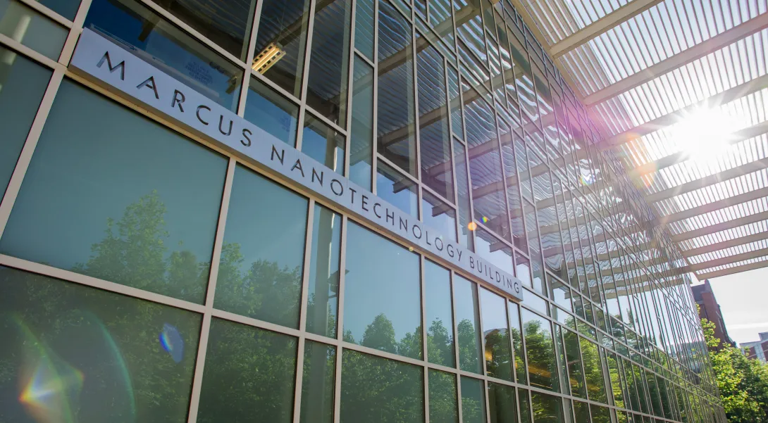
Through the Institute of Matter and Systems’ core facilities, housed in the Marcus Nanotechnology Building, DISC will accelerate semiconductor and advanced packaging development.
“The awarding of the Digital Twin Manufacturing USA Institute is a culmination of more than three years of work with the Semiconductor Research Corporation and other valued team members who share a similar vision of advancing U.S. leadership in semiconductors and advanced packaging,” said George White, senior director for strategic partnerships at Georgia Tech.
“As a founding member of the SMART USA Institute, Georgia Tech values this long-standing partnership. Its industry and academic partners, including the HBCU CHIPS Network, stand ready to make significant contributions to realize the goals and objectives of the SMART USA Institute,” White added.
Georgia Tech also plans to capitalize on the supply chain and optimization strengths of the No. 1-ranked H. Milton Stewart School of Industrial and Systems Engineering (ISyE). ISyE experts will help develop supply-chain digital twins to optimize and streamline manufacturing and operational efficiencies.
David Henshall, SRC vice president of Business Development, said, “The SMART USA Institute will advance American digital twin technology and apply it to the full semiconductor supply chain, enabling rapid process optimization, predictive maintenance, and agile responses to chips supply chain disruptions. These efforts will strengthen U.S. global competitiveness, ensuring our country reaps the rewards of American innovation at scale.”
News Contact
Amelia Neumeister | Research Communications Program Manager
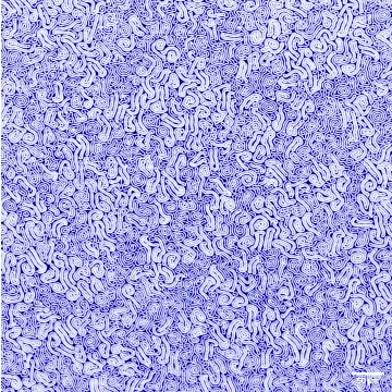
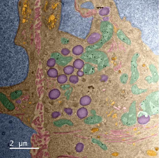

The National Nanotechnology Coordinated Infrastructure (NNCI) announced the winners of the 2024 image contest. The contest, Plenty of Beauty at the Bottom, celebrates the beauty of the micro and nanoscale.
Sites from across the NNCI contributed stunning, unique, and whimsical images of the micro and nanoscale for the 2024 image contest. The public cast over 2,100 votes to determine this year’s winners. First place winning artists will receive up to $1,000 in travel support to a professional conference of their choice and their sites receive a framed print of their winning image. Honorable mentions will receive a framed print of their image.
News Contact
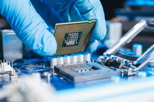
The National Science Foundation has awarded $2 million to Clark Atlanta University in partnership with the HBCU CHIPS Network, a collaborative effort involving historically black colleges and universities (HBCUs), government agencies, academia, and industry that will serve as a national resource for semiconductor research and education.
“This is an exciting time for the HBCU CHIPS Network,” said George White, senior director for Strategic Partnerships at Georgia Tech. “This funding, and the support of Georgia Tech Executive Vice President for Research Chaouki Abdallah, is integral for the successful launch of the CHIPS Network.”
The HBCU Chips Network works to cultivate a diverse and skilled workforce that supports the national semiconductor industry. The student research and internship opportunities along with the development of specialized curricula in semiconductor design, fabrication, and related fields will expand the microelectronics workforce. As part of the network, Georgia Tech will optimize the packaging of chips into systems.
News Contact
Georgia Tech Contact:
Amelia Neumeister | Research Communications Program Manager
Clark Atlanta University Contact:
Frances Williams

Ankur Singh has developed a new way of programming T cells that retains their naïve state, making them better fighters. — Photo by Jerry Grillo
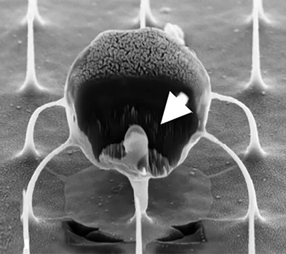
This is an image of a T cell on a nanowire array. The arrow indicates where a nanowire has penetrated the cell, delivering therapeutic miRNA.
Adoptive T-cell therapy has revolutionized medicine. A patient’s T-cells — a type of white blood cell that is part of the body’s immune system — are extracted and modified in a lab and then infused back into the body, to seek and destroy infection, or cancer cells.
Now Georgia Tech bioengineer Ankur Singh and his research team have developed a method to improve this pioneering immunotherapy.
Their solution involves using nanowires to deliver therapeutic miRNA to T-cells. This new modification process retains the cells’ naïve state, which means they’ll be even better disease fighters when they’re infused back into a patient.
“By delivering miRNA in naïve T cells, we have basically prepared an infantry, ready to deploy,” Singh said. “And when these naïve cells are stimulated and activated in the presence of disease, it’s like they’ve been converted into samurais.”
Lean and Mean
Currently in adoptive T-cell therapy, the cells become stimulated and preactivated in the lab when they are modified, losing their naïve state. Singh’s new technique overcomes this limitation. The approach is described in a new study published in the journal Nature Nanotechnology.
“Naïve T-cells are more useful for immunotherapy because they have not yet been preactivated, which means they can be more easily manipulated to adopt desired therapeutic functions,” said Singh, the Carl Ring Family Professor in the Woodruff School of Mechanical Engineering and the Wallace H. Coulter Department of Biomedical Engineering.
The raw recruits of the immune system, naïve T-cells are white blood cells that haven’t been tested in battle yet. But these cellular recruits are robust, impressionable, and adaptable — ready and eager for programming.
“This process creates a well-programmed naïve T-cell ideal for enhancing immune responses against specific targets, such as tumors or pathogens,” said Singh.
The precise programming naïve T-cells receive sets the foundational stage for a more successful disease fighting future, as compared to preactivated cells.
Giving Fighter Cells a Boost
Within the body, naïve T-cells become activated when they receive a danger signal from antigens, which are part of disease-causing pathogens, but they send a signal to T-cells that activate the immune system.
Adoptive T-cell therapy is used against aggressive diseases that overwhelm the body’s defense system. Scientists give the patient’s T-cells a therapeutic boost in the lab, loading them up with additional medicine and chemically preactivating them.
That’s when the cells lose their naïve state. When infused back into the patient, these modified T-cells are an effective infantry against disease — but they are prone to becoming exhausted. They aren’t samurai. Naïve T-cells, though, being the young, programmable recruits that they are, could be.
The question for Singh and his team was: How do we give cells that therapeutic boost without preactivating them, thereby losing that pristine, highly suggestable naïve state? Their answer: Nanowires.
NanoPrecision: The Pointed Solution
Singh wanted to enhance naïve T-cells with a dose of miRNA. miRNA is a molecule that, when used as a therapeutic, works as a kind of volume knob for genes, turning their activity up or down to keep infection and cancer in check. The miRNA for this study was developed in part by the study’s co-author, Andrew Grimson of Cornell University.
“If we could find a way to forcibly enter the cells without damaging them, we could achieve our goal to deliver the miRNA into naïve T cells without preactivating them,” Singh explained.
Traditional modification in the lab involves binding immune receptors to T-cells, enabling the uptake of miRNA or any genetic material (which results in loss of the naïve state). “But nanowires do not engage receptors and thus do not activate cells, so they retain their naïve state,” Singh said.
The nanowires, silicon wafers made with specialized tools at Georgia Tech’s Institute for Electronics and Nanotechnology, form a fine needle bed. Cells are placed on the nanowires, which easily penetrate the cells and deliver their miRNA over several hours. Then the cells with miRNA are flushed out from the tops of the nanowires, activated, eventually infused back into the patient. These programmed cells can kill enemies efficiently over an extended time period.
“We believe this approach will be a real gamechanger for adoptive immunotherapies, because we now have the ability to produce T-cells with predictable fates,” says Brian Rudd, a professor of immunology at Cornell University, and co-senior author of the study with Singh.
The researchers tested their work in two separate infectious disease animal models at Cornell for this study, and Singh described the results as “a robust performance in infection control.”
In the next phase of study, the researchers will up the ante, moving from infectious disease to test their cellular super soldiers against cancer and move toward translation to the clinical setting. New funding from the Georgia Clinical & Translational Science Alliance is supporting Singh’s research.
CITATION: Kristel J. Yee Mon, Sungwoong Kim, Zhonghao Dai, Jessica D. West, Hongya Zhu5, Ritika Jain, Andrew Grimson, Brian D. Rudd, Ankur Singh. “Functionalized nanowires for miRNA-mediated therapeutic programming of naïve T cells,” Nature Nanotechnology.
FUNDING: Curci Foundation, NSF (EEC-1648035, ECCS-2025462, ECCS-1542081), NIH (5R01AI132738-06, 1R01CA266052-01, 1R01CA238745-01A1, U01CA280984-01, R01AI110613 and U01AI131348).
News Contact
Jerry Grillo

The Biden-Harris Administration announced that the U.S. Department of Commerce and Absolics, an affiliate of the Korea-based SKC, have signed a non-binding preliminary memorandum of terms to provide up to $75 million in direct funding under the CHIPS and Science Act to help advance U.S. technology leadership. The proposed investment would support the construction of a 120,000 square-foot facility in Covington, Georgia and the development of substrates technology for use in semiconductor advanced packaging. Started through a collaboration with the 3D Packaging Research Center at Georgia Tech, Absolics’ project serves as an example of American lab-to-fab development and production.
"Glass-core packaging holds the promise to revolutionize the field of advanced packaging and impact major paradigms such as artificial intelligence, mm-wave/THz communication, and photonic connectivity," said Muhannad Bakir, Dan Fielder Professor in the School of Electrical and Computer Engineering and Director of the 3D Systems Packaging Research Center at Georgia Tech. "We look forward to supporting Absolics in establishing a glass-core packaging facility in the State of Georgia through workforce development initiatives."
Because of President Biden’s CHIPS and Science Act, this proposed investment would support over an estimated 1,000 construction jobs and approximately 200 manufacturing and R&D jobs in Covington and enhance innovation capacity at Georgia Institute of Technology, supporting the local semiconductor talent pipeline.
The proposed investment with Absolics is the first proposed CHIPS investment in a commercial facility supporting the semiconductor supply chain by manufacturing a new advanced material.
News Contact
Amelia Neumeister
Research Communications Program Manager


When Amy Bonecutter-Leonard was a second-semester undergraduate at the Georgia Institute of Technology, she applied for a work-study job in the cleanroom at the Microelectronics Research Center (MiRC). There, she learned process techniques for making the same type of electronic chips used in cellphones.
With this new knowledge, she could train and help other students with their research. At the time, Bonecutter-Leonard was a chemical engineering major with no plans to go into microelectronics. Working in the cleanroom changed that.
“I fell in love with microelectronics through exposure to the research and development work performed in the cleanroom,” she said.
What started as a student job led to her taking microelectronics classes — and eventually to a career in the field. “My work-study prepared me with hands-on technical skills I would have never learned from just being in a classroom,” she said. Now, Bonecutter-Leonard works as a microelectronics business chief engineer at defense contractor L3Harris Technologies.
Her story is one of many from the Institute for Electronics and Nanotechnology (IEN, the successor to MiRC), which has been training students from kindergarten to graduate school to be leaders in the microelectronics and nanotechnology space. The goal of IEN’s outreach is to make nanotechnology and microelectronics — such as computer chips and sensors — as accessible as any other science. Ultimately, these efforts will build up the U.S. workforce in the field, ensuring the country remains at the forefront of the technology that powers Americans’ everyday lives.
Building the Workforce
Bolstering the number of workers in the microelectronics industry is imperative to keep the U.S. globally competitive. Right now, 40% of the industry's labor force is older than 50, with practitioners aging out of their careers at a pace new talent cannot match. Additionally, heavy educational barriers to entry, including required degrees and specialized training, prevent more people from pursuing careers in the field. Without dedicated efforts, the entire sector — and the nation — will fall behind.
IEN is working to solve this pipeline problem.
“With the national semiconductor workforce aging, it is important now more than ever that we educate the next generation to move into these jobs,” said Michael Filler, IEN’s interim executive director. “IEN is proud to support the semiconductor industry by providing students with the interdisciplinary skills and hands-on technical training essential for success in this fast-paced, global field.”
Georgia Tech is uniquely positioned to lead this charge with its 28,500 square feet of academic cleanroom space, the largest in the Southeast and among the largest in the U.S. From micro-electro-mechanical systems to electronics fabrication, workers have 100 bays in which to conduct leading-edge research. These cleanrooms are also key teaching and training facilities.
IEN invites anyone from around the world, whether affiliated with the Institute or not, to become a core user of the cleanroom facilities. The center also regularly hosts short courses for external partners — academic, industry, and government — in microfabrication and soft lithography for microfluidics. Over the past three years, more than 700 people went through new-user orientation, and 193 enrolled in the short courses.
Teaching the Next Generation
Making nanotechnology — of which microelectronics is an example — educationally accessible begins before college. Each semester, more than 800 K-12 students participate in IEN’s Introduction to Nanotechnology virtual lesson. Associate Director for Education and Outreach Mikkel Thomas begins his presentations by asking a simple question: What do you know about nanotechnology?
“About 99% of the time, they say that’s what makes Ironman’s suit work,” said Thomas. “That means they’ve learned the wrong lesson — that nanotechnology is a futuristic tech and that you have to be as smart as Tony Stark to work in the field.
“But most people interact with nanotechnology multiple times throughout their day, and they have no idea they're doing it.”
Thomas also emphasizes there is a career path for everyone, even if they don’t plan to get a traditional four-year degree. Part of IEN’s workforce development initiative is to build up the entire pipeline from industry and research lab technicians at the certificate level to postdoctoral researchers.
“It’s important for us to reach kids who don’t know what career options are available in nanotechnology,” Thomas said. “We want them to know that whatever they're interested in, there is a pathway for them.”
Sixth- through eighth-grade students sparked by this conversation can attend Chip Camp, a three-day STEM summer camp sponsored by Micron. They begin with a day at IEN to learn about thin films, magic sands, ferrofluids, and measuring their height in nanometers. The rest of the camp features hands-on visits to the Materials Characterization Facility (MCF) and the IEN cleanroom, where they can try on the white “bunny suits” technicians wear in the lab.
To further their reach, IEN’s workforce development team collaborates with teachers to bring nanotechnology into classrooms. During the summer, IEN offers the Research Experience for Teachers, a training program for public school and community college teachers to conduct nanotechnology research and learn how to incorporate it into their lessons. Middle school teachers have similar opportunities through the Nanoscience Summer Institute for Middle School Teachers.
Training the Workforce
When these students get to a university like Georgia Tech, IEN hires them for work-study jobs like the one Bonecutter-Leonard had. The hands-on cleanroom training is also vital to graduate students pursuing advanced degrees.
Katie Young earned her Ph.D. in materials science and engineering at Georgia Tech. Learning her way around the IEN cleanroom was essential for her graduate studies.
“My dissertation research involved synthesizing two-dimensional materials — only a single atom thick — for permeation barriers,” she explained. “I often used the cleanroom’s vacuum systems to synthesize and process 2D materials.” Now a research scientist at the Georgia Tech Research Institute, Young still works in the cleanroom on semiconductor device fabrication, building prototype quantum and biological sensors.
IEN opportunities are not limited to graduate research. Annually, about 150 Georgia Tech undergraduate students take microelectronics packaging and devices classes, with labs taught by IEN staff in the teaching cleanroom. These courses include Integrated Circuit Fabrication (ECE 4452), in which students learn to fabricate circuit elements, and the Science and Engineering of Microelectronic Fabrication (ChBE 4050/6050, open to graduate students as well), for students interested in semiconductor materials and fabrication.
Students don’t need to enroll at Georgia Tech to benefit from training, courses, and other opportunities. IEN’s internship program provides technical college students with training to become microelectronics technicians, either through work in the Biocleanroom or in the MCF.
Empowering Future Innovators
IEN also participates in the National Science Foundation Research Experiences for Undergraduates (REU), which provides opportunities for students from underrepresented groups or who attend schools without similar facilities. While enrolled at another university, John Mark Page was introduced to Georgia Tech’s cleanroom through an REU.
“That was my first exposure to any facility of this kind, and it felt like I was looking at the future. Being in a facility that can fabricate devices at or near the atomic level — it was hard to fathom,” Page said. “I had never thought that participating in microelectronics and nanotechnology as a student, especially as an undergraduate, was something I could do.”
As a result of his REU, Page transferred to Georgia Tech — he will graduate this summer with a bachelor’s degree in electrical engineering. He also completed a second REU at the University of North Carolina at Chapel Hill, worked as a student assistant in the IEN cleanroom, and participated in a Vertically Integrated Project (VIP), Chip Scale Power and Energy.
“I was interested in the VIP because it allowed me to spend more time in the cleanroom, familiarizing myself with semiconductor fabrication methods and training on new fabrication equipment,” Page explained. His experiences inspired him to consider a future career in the semiconductor industry.
“It wasn’t only the 10-week experience of the REU that made a lasting impact on me,” he said. “It was also the relationships formed with the people of IEN. The staff there are exceptional representatives of Georgia Tech, and they make IEN a tremendous asset to the future of microelectronics and nanotechnology in the U.S.”
Biya Haile, an ECE Ph.D. student, had a similarly meaningful REU experience. Haile, whose research focuses on creating micro-electro-mechanical systems-based sensors (MEMS), described the REU as “immersive.”
“The REU project enabled me to study chemical micro-sensor technologies, as well as state-of-the-art additive nano-manufacturing techniques, which has contributed to my research,” he said. “I feel lucky that my academic journey has entailed developing new technologies that use nanoscience to solve big problems.”
While Haile is currently focused more on designing and testing rapid processes for fabricating MEMS-based devices, he still occasionally works in the cleanroom on fabrication. He plans to go into the microelectronics industry after graduating.
The Path Ahead
All of IEN’s training and educational offerings align with IEN’s mission to bolster and diversify the microelectronics workforce, according to George White, senior director of strategic partnerships for the Georgia Tech research enterprise. “IEN has been at the forefront of the CHIPS infrastructure buildout, particularly in the area of education and workforce development,” he noted.
IEN’s efforts impact not just Atlanta but the entire country. Georgia Tech’s leadership in microelectronics research trains the innovators and practitioners of the future everywhere and ensures that America stays at the forefront of leading-edge technology. As demand increases for microelectronics, IEN is moving to meet it.
Effective July 1, 2024, the Institute for Electronics and Nanotechnology and the Institute for Materials will evolve into the Institute for Matter and Systems (IMS). This strategic union aims to foster convergent research at Georgia Tech, focusing on the science, technology, and societal underpinnings of cutting-edge materials and devices. Eric Vogel will be the director of IMS, and Michael Filler will be the deputy director.
News Contact
Media Contact: Tess Malone, Senior Research Writer/Editor tess.malone@gatech.edu

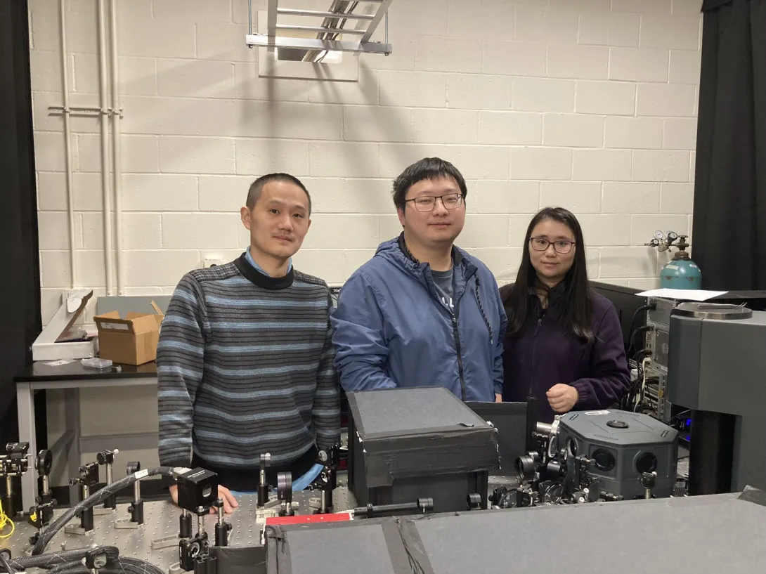
Quantum sensors detect the smallest of environmental changes — for example, an atom reacting to a magnetic field. As these sensors “read” the unique behaviors of subatomic particles, they also dramatically improve scientists’ ability to measure and detect changes in our wider environment.
Monitoring these tiny changes results in a wide range of applications — from improving navigation and natural disaster forecasting, to smarter medical imaging and detection of biomarkers of disease, gravitational wave detection, and even better quantum communication for secure data sharing.
Georgia Tech physicists are pioneering new quantum sensing platforms to aid in these efforts. The research team’s latest study, “Sensing Spin Wave Excitations by Spin Defects in Few-Layer Thick Hexagonal Boron Nitride” was published in Science Advances this week.
The research team includes School of Physics Assistant Professors Chunhui (Rita) Du and Hailong Wang (corresponding authors) alongside fellow Georgia Tech researchers Jingcheng Zhou, Mengqi Huang, Faris Al-matouq, Jiu Chang, Dziga Djugba, and Professor Zhigang Jiang and their collaborators.
An ultra-sensitive platform
The new research investigates quantum sensing by leveraging color centers — small defects within crystals (Du’s team uses diamonds and other 2D layered materials) that allow light to be absorbed and emitted, which also give the crystal unique electronic properties.
By embedding these color centers into a material called hexagonal boron nitride (hBN), the team hoped to create an extremely sensitive quantum sensor — a new resource for developing next-generation, transformative sensing devices.
For its part, hBN is particularly attractive for quantum sensing and computing because it could contain defects that can be manipulated with light — also known as "optically active spin qubits."
The quantum spin defects in hBN are also very magnetically sensitive, and allow scientists to “see” or “sense” in more detail than other conventional techniques. In addition, the sheet-like structure of hBN is compatible with ultra-sensitive tools like nanodevices, making it a particularly intriguing resource for investigation.
The team’s research has resulted in a critical breakthrough in sensing spin waves, Du says, explaining that “in this study, we were able to detect spin excitations that were simply unattainable in previous studies.”
Detecting spin waves is a fundamental component of quantum sensing, because these phenomena can travel for long distances, making them an ideal candidate for energy-efficient information control, communication, and processing.
The future of quantum
“For the first time, we experimentally demonstrated two-dimensional van der Waals quantum sensing — using few-layer thick hBN in a real-world environment,” Du explains, underscoring the potential the material holds for precise quantum sensing. “Further research could make it possible to sense electromagnetic features at the atomic scale using color centers in thin layers of hBN.”
Du also emphasizes the collaborative nature of the research, highlighting the diverse skill sets and resources of researchers within Georgia Tech.
“Within the School of Physics, Professor Zhigang Jiang's research group provided the team with high-quality hBN crystals. Jingcheng Zhou, who is a member of both Professor Hailong Wang’s and my research teams, performed the cutting-edge quantum sensing measurements,” she says. “Many incredible students also helped with this project.”
Du is a leading scientist in the field of quantum sensing — this year, she received a new grant from the U.S. Department of Energy, along with a Sloan Research Fellowship for her pioneering work on developing state-of-the-art quantum sensing techniques for quantum information technology applications. The prestigious Sloan award recognizes researchers whose “creativity, innovation, and research accomplishments make them stand out as the next-generation of leaders in the fields.”
This work is supported by the U. S. National Science Foundation (NSF) under award No. DMR-2342569, the Air Force Office of Scientific Research under award No. FA9550-20-1-0319 and its Young Investigator Program under award No. FA9550-21-1-0125, the Office of Naval Research (ONR) under grant No. N00014-23-1-2146, NASA-REVEALS SSERVI (CAN No. NNA17BF68A), and NASA-CLEVER SSERVI (CAN No. 80NSSC23M0229).
News Contact
Written by Selena Langner
Contact: Jess Hunt-Raston
Director of Communications
College of Sciences at Georgia Tech

Effective July 1, Eric Vogel will become the executive director of the Institute for Matter and Systems (IMS), Georgia Tech’s newest Interdisciplinary Research Institute (IRI) that will launch on the same date.
As an evolution of the Institute for Materials (IMat) and the Institute for Electronics and Nanotechnology (IEN), IMS aims to enable convergent research at Georgia Tech related to the science, technology, and societal underpinnings of innovative materials and devices. Additionally, IMS seeks to integrate these innovations into systems that enhance human well-being and performance across information and communication, the built environment, and human-centric technologies that improve human health, wellness, and performance.
“Executive Vice President for Research Chaouki Abdallah and I are very excited about the launch of IMS, which positions Georgia Tech for integration of science and technology from atoms to devices, while explicitly drawing in researchers in the social sciences, design, business, and computing,” said Vice President of Interdisciplinary Research Julia Kubanek.
“IMS will ensure relevance across Georgia Tech through its newly configured Internal Advisor and Ambassador Board with representation across all six Colleges and GTRI,” she said. “Additional advisory committees representing IMS employees and facility users will ensure that we don’t sacrifice any of the research excellence for which IEN and IMat are known. With IMS I expect we will be even better positioned to tackle research problems that will have the greatest positive societal impact.”
Vogel will continue in his current position as the executive director of IMat until the launch of IMS. In addition to leading and growing IMat, Vogel is the Hightower Professor of Materials Science and Engineering at Georgia Tech’s School of Materials Science and Engineering, and he served as the IEN deputy director prior to leading IMat.
“It is an honor to be appointed executive director of the Institute for Matter and Systems, and I look forward to collaborating with the talented faculty and staff associated with it,” said Vogel. “This opportunity allows us to leverage the core competencies of IEN and IMat while extending our capabilities beyond nanotechnology and materials science. Together, we will be a hub for interdisciplinary research ranging from advanced materials to complex systems that solve global challenges.”
Georgia Tech’s IRIs facilitate collaboration between researchers and students from its six Colleges, the Georgia Tech Research Institute, national laboratories, and corporate entities to tackle critical topics of strategic significance for the Institute as well as for local, state, national, and international communities. IMS will also house and maintain the state-of-the-art Materials Characterization Facility and one of the largest academic cleanrooms in the nation, which offers a broad range of fabrication capabilities from basic discovery to prototype realization.
Before joining Georgia Tech in 2011, Vogel was an associate professor of materials science and engineering and electrical engineering at the University of Texas at Dallas. During this time, he also served as the associate director of the Texas Analog Center of Excellence and led UT Dallas’s involvement in the Southwest Academy for Nanoelectronics.
Prior to UT Dallas, he led the CMOS and Novel Devices Group and established the Nanofabrication Facility at the National Institute of Standards and Technology. Vogel holds a Ph.D. in electrical engineering from North Carolina State University and a B.S. in electrical engineering from the Pennsylvania State University. His research focuses on the development and fundamental understanding of electronic and nanomaterials and devices.
News Contact
Laurie Haigh
Research Communications