

Energy is everywhere, affecting everything, all the time. And it can be manipulated and converted into the kind of energy that we depend on as a civilization. But transforming this ambient energy (the result of gyrating atoms and molecules) into something we can plug into and use when we need it requires specific materials.
These energy materials — some natural, some manufactured, some a combination — facilitate the conversion or transmission of energy. They also play an essential role in how we store energy, how we reduce power consumption, and how we develop cleaner, efficient energy solutions.
“Advanced materials and clean energy technologies are tightly connected, and at Georgia Tech we’ve been making major investments in people and facilities in batteries, solar energy, and hydrogen, for several decades,” said Tim Lieuwen, the David S. Lewis Jr. Chair and professor of aerospace engineering, and executive director of Georgia Tech’s Strategic Energy Institute (SEI).
That research synergy is the underpinning of Georgia Tech Energy Materials Day (March 27), a gathering of people from academia, government, and industry, co-hosted by SEI, the Institute for Materials (IMat), and the Georgia Tech Advanced Battery Center. This event aims to build on the momentum created by Georgia Tech Battery Day, held in March 2023, which drew more than 230 energy researchers and industry representatives.
“We thought it would be a good idea to expand on the Battery Day idea and showcase a wide range of research and expertise in other areas, such as solar energy and clean fuels, in addition to what we’re doing in batteries and energy storage,” said Matt McDowell, associate professor in the George W. Woodruff School of Mechanical Engineering and the School of Materials Science and Engineering (MSE), and co-director, with Gleb Yushin, of the Advanced Battery Center.
Energy Materials Day will bring together experts from academia, government, and industry to discuss and accelerate research in three key areas: battery materials and technologies, photovoltaics and the grid, and materials for carbon-neutral fuel production, “all of which are crucial for driving the clean energy transition,” noted Eric Vogel, executive director of IMat and the Hightower Professor of Materials Science and Engineering.
“Georgia Tech is leading the charge in research in these three areas,” he said. “And we’re excited to unite so many experts to spark the important discussions that will help us advance our nation’s path to net-zero emissions.”
Building an Energy Hub
Energy Materials Day is part of an ongoing, long-range effort to position Georgia Tech, and Georgia, as a go-to location for modern energy companies. So far, the message seems to be landing. Georgia has had more than $28 billion invested or announced in electric vehicle-related projects since 2020. And Georgia Tech was recently ranked by U.S. News & World Report as the top public university for energy research.
Georgia has become a major player in solar energy, also, with the announcement last year of a $2.5 billion plant being developed by Korean solar company Hanwha Qcells, taking advantage of President Biden’s climate policies. Qcells’ global chief technology officer, Danielle Merfeld, a member of SEI’s External Advisory Board, will be the keynote speaker for Energy Materials Day.
“Growing these industry relationships, building trust through collaborations with industry — these have been strong motivations in our efforts to create a hub here in Atlanta,” said Yushin, professor in MSE and co-founder of Sila Nanotechnologies, a battery materials startup valued at more than $3 billion.
McDowell and Yushin are leading the battery initiative for Energy Materials Day and they’ll be among 12 experts making presentations on battery materials and technologies, including six from Georgia Tech and four from industry. In addition to the formal sessions and presentations, there will also be an opportunity for networking.
“I think Georgia Tech has a responsibility to help grow a manufacturing ecosystem,” McDowell said. “We have the research and educational experience and expertise that companies need, and we’re working to coordinate our efforts with industry.”
Marta Hatzell, associate professor of mechanical engineering and chemical and biomolecular engineering, is leading the carbon-neutral fuel production portion of the event, while Juan-Pablo Correa-Baena, assistant professor in MSE, is leading the photovoltaics initiative.
They’ll be joined by a host of experts from Georgia Tech and institutes across the country, “some of the top thought leaders in their fields,” said Correa-Baena, whose lab has spent years optimizing a semiconductor material for solar energy conversion.
“Over the past decade, we have been working to achieve high efficiencies in solar panels based on a new, low-cost material called halide perovskites,” he said. His lab recently discovered how to prevent the chemical interactions that can degrade it. “It’s kind of a miracle material, and we want to increase its lifespan, make it more robust and commercially relevant.”
While Correa-Baena is working to revolutionize solar energy, Hatzell’s lab is designing materials to clean up the manufacturing of clean fuels.
“We’re interested in decarbonizing the industrial sector, through the production of carbon-neutral fuels,” said Hatzell, whose lab is designing new materials to make clean ammonia and hydrogen, both of which have the potential to play a major role in a carbon-free fuel system, without using fossil fuels as the feedstock. “We’re also working on a collaborative project focusing on assessing the economics of clean ammonia on a larger, global scale.”
The hope for Energy Materials Day is that other collaborations will be fostered as industry’s needs and the research enterprise collide in one place — Georgia Tech’s Exhibition Hall — over one day. The event is part of what Yushin called “the snowball effect.”
“You attract a new company to the region, and then another,” he said. “If we want to boost domestic production and supply chains, we must roll like a snowball gathering momentum. Education is a significant part of that effect. To build this new technology and new facilities for a new industry, you need trained, talented engineers. And we’ve got plenty of those. Georgia Tech can become the single point of contact, helping companies solve the technical challenges in a new age of clean energy.”
News Contact
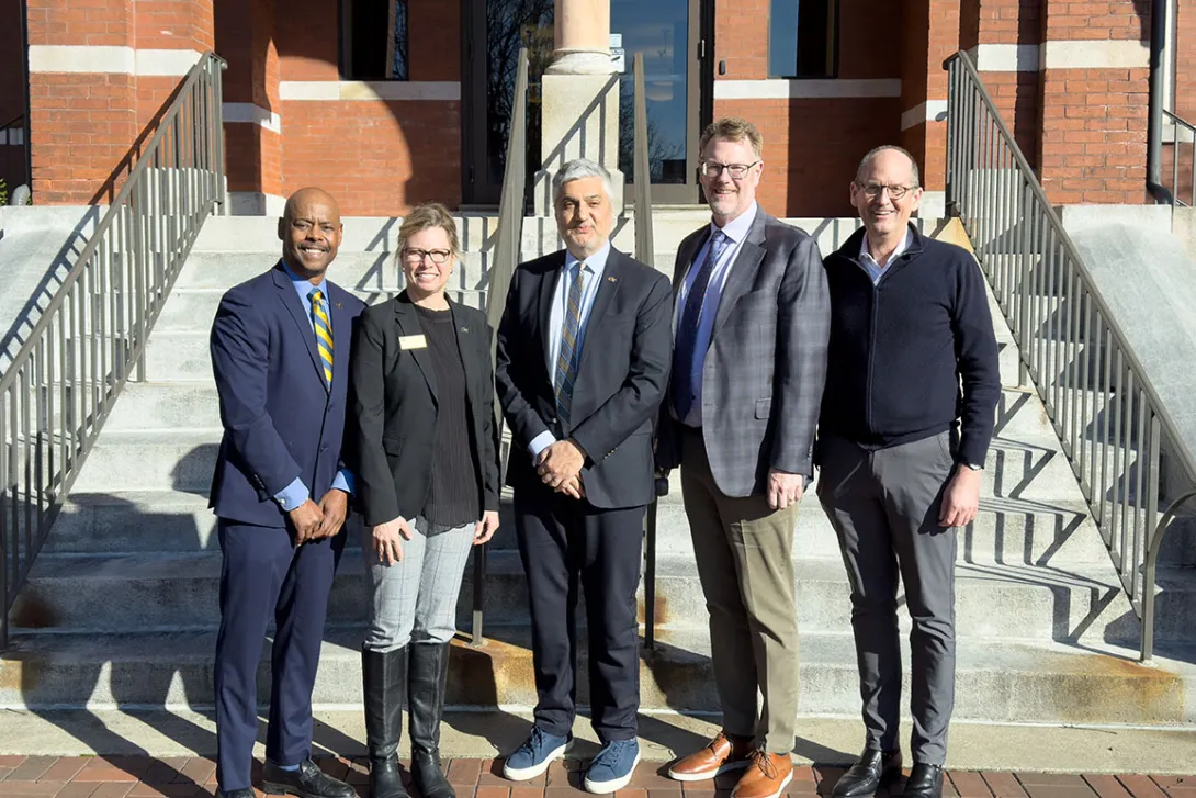
From Left: George White, Julia Kubanek, Chaouki T. Abdallah, Scott DeBoer, Steve McLaughlin
The Georgia Institute of Technology today announced the signing of a master research agreement with Micron Technology, a global leader in memory and storage solutions. Under the new agreement, the two organizations will expand their collaborative efforts in providing students with experiential research opportunities and expanding access to engineering education.
“We are proud to join forces with Georgia Tech, home to some of the nation’s top programs, to expand students’ opportunities in STEM education,” said Scott DeBoer, executive vice president of Technology and Products at Micron. “This collaboration will help push the boundaries in memory technology innovation and ensure we prepare the workforce of the future.”
“We believe that when academia and industry converge, the best ideas flourish into game-changing innovations,” said Chaouki T. Abdallah, executive vice president for Research at Georgia Tech. “The synergy between Micron and Georgia Tech has already been tremendously fruitful, and we are so excited for the boundless opportunities on our shared horizon.”
“The signing of the master research agreement represents a significant step towards increasing additional collaboration pathways between Micron and GT including the joint pursuit of major federal funding activities, technology transfer, student internships and technology transfer,” said George White, senior director of Strategic Partnerships at Georgia Tech.
The first project under the agreement is already underway. Saibal Mukhopadhyay, professor in the School of Electrical and Computer Engineering, is leading the research efforts titled “Configurable Processing-In-Memory.” This cutting-edge research will enable memory devices to work faster and more efficiently.
News Contact

Researchers have documented for the first time the stresses that build up around solid-state battery electrolytes, helping set the stage for the development of improved and more efficient batteries. Scientists have long thought that stresses can build up around dendrites, thin metallic projects that can ultimately short out solid-electrolyte batteries, but they haven’t been precisely measured.
A team of scientists at Georgia Tech, Brown University, Nanyang Technological University, and MIT have measured the mechanical stresses that develop in dendrites – solving a long-standing hypothesis that high stresses can be developed around dendrites. Dendrites pierce through solid electrolytes, eventually crossing from one electrode to the other and shorting out the solid-state battery cell.
Georgia Tech Professor Christos Athanasiou and the multidisciplinary team used photoelasticity to measure the stress on batteries caused during the battery cycle. In their paper, Operando Measurements of Dendrite-Induced Stresses in Ceramic Electrolytes using Photoelasticity, they managed to overcome challenges associated with measurements of easy to break, very tiny solid electrolyte samples. The samples thickness was about 10 times smaller than the average diameter of human hair.
The team used an old - and almost forgotten - principle of photoelasticity to directly measure the stress fields during cell operation. Photoelasticity’s contactless nature also allows for the stresses to be directly measured and visualized at the dendrite tips. By shining light through the material under a special photoelastic microscope, it revealed intricate stress fields. In this case, the stress revealed from passing light through the electrolyte appeared at the tip of the propagation dendrite.
This advanced experimental setup has set the stage for profound exploration of stresses developed during battery operation across various electrolytes and conditions, revealing critical data on loading conditions and the dynamics of lithium metal penetration events.
This is just one example where creative, yet simple experimentation, can lead to fundamental discoveries. The Daedalus Lab at Georgia Tech, inspired by the ingenuity of its namesake, the mythical Greek inventor, is dedicated to decarbonizing the future through the development and promotion of sustainable materials and structures, utilizing innovative experimental approaches and artificial intelligence.
News Contact
Kelsey Gulledge
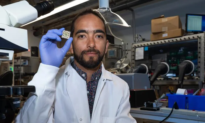
Juan-Pablo Correa-Baena leads the Materials for Solar Energy Harvesting and Conversion research initiative for the Institute for Materials (IMat) and Strategic Energy Institute at Georgia Tech. In this role, he is working to create a community around solar energy harvesting and conversion at Georgia Tech. He aims to integrate photovoltaic, photodetectors, and related devices into IMaT-related research; energize research in these areas at Georgia Tech at large; and consolidate the expertise of the many research groups working on or around photovoltaics/photodetectors that will allow researchers to target interdisciplinary research funding opportunities. He is also an assistant professor and the Goizueta Junior Faculty Rotating Chair in the School of Materials Science and Engineering.
In this brief Q&A, Correa-Baena discusses his research focus, how it relates to materials research, and the impact of this initiative.
What is your field of expertise and at what point in your life did you first become interested in this area?
I am an expert in materials for energy harvesting and conversion. I first became interested in this topic when I was an undergraduate student and started thinking about the future of energy production.
What questions or challenges sparked your current materials research?
I was born and raised in a country where fossil fuels dominate the energy production landscape, yet where renewables are readily available. Colombia is a large producer of oil but also boasts a huge potential for solar energy production. This juxtaposition always puzzled me growing up. As a researcher in this field, I want to ensure that all countries around the world have access to solar energy, by helping lower deployment cost.
Why is your initiative important to the development of Georgia Tech’s Materials research strategy?
There is a growing need to expand our research footprint at Georgia Tech with regard to photovoltaics. This is especially important with the impact of the photovoltaic industry presence in Georgia. My initiative is focusing on galvanizing activities around photovoltaic research at Georgia Tech that can benefit our footprint globally as well as locally with industry partners.
What are the broader global and social benefits of the research you and your team conduct?
The main benefit of the research we do is to the photovoltaic industry, which we hope to engage through cutting-edge research at Georgia Tech.
What are your plans for engaging a wider Georgia Tech faculty pool with IMat research?
I am planning to organize an internal workshop, as well as a session on photovoltaics in the Next Generation of Energy Materials Symposium to be held in March 2024 at Georgia Tech. In addition, as part of my efforts to engage the Georgia Tech community at large, I am working to create a website that will connect the Georgia Tech community working towards advancing photovoltaic capabilities for future manufacturing advancements.
News Contact
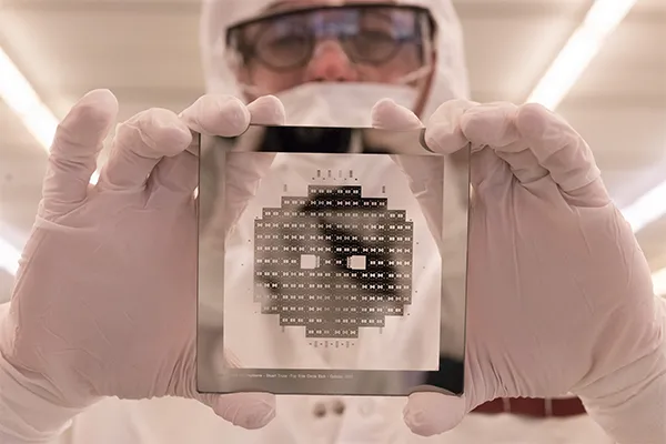
Left to right: Arijit Raychowdhury, Victor Fung, Jennifer Hasler, Michael Filler, Chip White

Semiconductors, or microchips, are vital to life in the modern world. They’re used in the microwave you heated your breakfast in this morning, the car you drove to work, the mobile phone you shouldn’t use while driving, the bank ATM you visited, and the screened device you’re reading this story on.
They’re in our TVs, refrigerators, and washing machines, helping us live comfortable lives. They also help us stay alive as part of the medical network, used in pacemakers, blood pressure monitors, and MRI machines, among other things. Also, our national economic and defense systems rely on them. Basically, semiconductors control and manage the flow of information in the machinery that keeps the world going.
And right now, at Georgia Tech, researchers are working to innovate chip technology to ensure that U.S. semiconductor development is globally competitive, reliable, sustainable, and resilient, today and in the future.
“If you look at semiconductors, or the whole area of computing, it spans across Georgia Tech — across many different schools and disciplines,” said Arijit Raychudhury, professor and Steve W. Chaddick Chair in the School of Electrical and Computer Engineering (ECE). “Starting with physics and chemistry, where we essentially learn how different types of materials will react, to materials science and engineering, to electrical engineering and computer engineering, to computer science.”
It's a diverse, multidisciplinary enterprise from bottom to top, Raychudhury noted. And there is still plenty of room at the bottom, as theoretical physicist Richard P. Feynman famously said more than 60 years ago, predicting that one day we’d be making things at the atomic level. We are. It’s a familiar realm to Victor Fung and his lab, where they are designing new materials for semiconductors from the ground up, atom by atom.
“We are interested in exploring how to translate the latest advances in AI and machine learning to aid in accelerating computational materials simulations and materials discovery,” said Fung, assistant professor in the School of Computational Science. “We’ve been developing methods which can accurately predict a wide range of materials’ properties, to greatly facilitate high-throughput materials screening.”
Fung’s lab is using AI to discover previously unstudied materials with the electronic properties to build into chips. This approach to creating “designer” semiconductors would be significantly faster and cover more of the materials space than current methods.
Improving the Landscape
Smaller, more efficient, and more powerful are all part of the constantly evolving landscape in semiconductor research and development. It’s a very expensive landscape. While many chips are about the size of a fingernail, they are among the most complex human-made objects on Earth. Just building a semiconductor fabrication factory costs billions of dollars.
For a chemical engineer like Michael Filler, that sounds like opportunity.
“Chemical engineers think about how we produce products on a massive scale,” said Filler, associate professor in the School of Chemical and Biomolecular Engineering and associate director of the Institute for Electronics and Nanotechnology (IEN).
Filler, whose research involves the growing of semiconductor components, like transistors, from seed particles, is aiming to help democratize the process of chip development, bringing down the cost substantially while maintaining performance. In a not too distant future, that could mean an individual at home printing a chip on a machine similar to a 3D printer.
“Imagine a laser printer that can literally spit out custom electronics in a matter of minutes,” Filler said. “We’re big believers in the individual’s ability to be creative and know what they want to build for their applications. Ultimately, we’re interested in giving makers and prototypers opportunities to customize electronics.”
He’s in the right place for the far-reaching research he has in mind, adding, “We are so blessed with great facilities at Georgia Tech. It would be hard to imagine working somewhere else, because very few places have the diversity and quality of tooling we have here.”
IEN, which facilitates much of the semiconductor research at Georgia Tech, is based in the Marcus Nanotechnology Building, with its state-of-the-art micro/nano fabrication facilities such as the shared cleanroom space and a laser machine lab for micromachining.
But it is the range of expertise and creativity among faculty and students who are making IEN and Georgia Tech a thought leader in semiconductor research. This is evidenced by Tech’s recent grant of $65.7 million from the Semiconductor Research Corporation and the Defense Research Projects Agency to launch two new interdisciplinary research centers.
Events like Georgia Tech Chip Day (May 2) and Nanowire Week, an international gathering happening in Atlanta in October, also speak to Tech’s growing influence in this area.
Answering the Call
The Covid-19 pandemic clarified just how difficult it can be to make more chips. A shortage of semiconductors affected the supply of phones, computers, and other commonly used items during the global shutdown. Increased demand, depleted reserves, and too few manufacturing plants and workers significantly crippled the supply chain.
“The high degree of geographic concentration in certain parts of the semiconductor supply chain has recently created a heightened risk of supply interruptions,” said Chip White, Schneider National Chair in Transportation and Logistics and professor in the H. Milton Stewart School of Industrial and Systems Engineering (ISyE). “Such interruptions and resulting wild fluctuations in semiconductor demand can threaten the nation’s public health, defense, and economic security.”
With that in mind, translational supply chain research is going on in several places on campus, White said, including the Supply Chain and Logistics Institute and the NSF AI Research Institute for Advances in Optimization. White and his colleagues are developing software platforms for stress testing manufacturing supply chains. The goal is to identify vulnerabilities and risk mitigation procedures to design and operate next generation supply chains for critical industries such as the semiconductor industry, to improve global competitiveness and strike a balance between market forces and national security.
In an effort to address and feed the next generation demand for chips, the Biden administration recently launched a massive effort to outcompete China in semiconductor manufacturing, offering $39 billion in funding incentives for companies seeking to build plants in the U.S.
Another related area of importance in the ongoing development of semiconductors is growing the workforce of the future, and that includes a new wave of researchers. This is a role that Jennifer Hasler takes seriously.
“I have a strong interest and belief in mentoring,” said Hasler, ECE professor and founder of the Integrated Computational Electronics lab at Georgia Tech. She’s proven, theoretically at least, that the technology already exists to build a silicon-based version of the human cerebral cortex (which would cost billions of dollars to design and build), but one of her favorite roles is working with new, young faculty.
“It’s a personal thing for me, but it’s one of the coolest things I’m involved in,” she said. “When they come to Georgia Tech, they see how big this place is, bigger than a company. I like to say to them, ‘Let’s calm down, take a breath, you’re good, so let’s go make some cool stuff. Let’s get some momentum going.’”
For Raychowdhury, director of the new Center for the Co-Design of Cognitive Systems (part of the JUMP 2.0 program), developing the skilled workforce of the future means answering the call of the nation.
“This is one of the largest ECE departments in the country, with many, many talented students,” he said. “And given the need and shortage of skilled professionals in this particular area, I think it’s critical for us to create that kind of pipeline.” Last year, ECE undergraduate students started taking a new, two-semester course, sponsored by Apple, in which they actually build microprocessors from scratch.
“This is completely new,” Raychowdhury said. “It’s expensive to offer this course, but we plan to keep doing it and we’re in conversations with other companies that want to invest in workforce development. So, in addition to doing fantastic research, we want to be sensitive to the needs of the country and a new generation.”
News Contact
Writer: Jerry Grillo
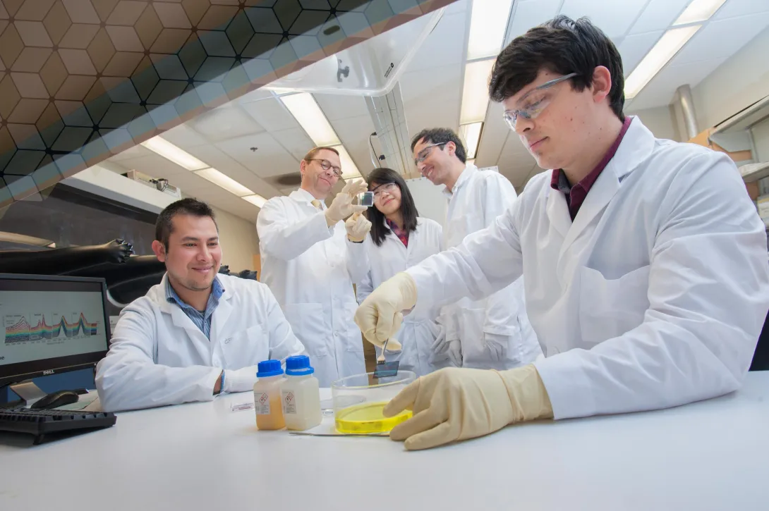
The Scalable Asymmetric Lifecycle Engagement Microelectronics Workforce Development program (SCALE) has announced the program will extend another five years and expand with $10.8 million additional Department of Defense (DoD) funding, with a ceiling of $99 million.
SCALE officials said this expansion of the nation’s preeminent program will further its goal to develop a next-generation workforce that can return the United States to prominence in global microelectronics manufacturing.
Georgia Tech participates in the partnership, which is led by Purdue University and managed by NSWC Crane. SCALE facilitates the training of highly skilled U.S. microelectronics engineers, hardware designers and manufacturing experts. SCALE brings together a public-private-academic partnership of 17 universities and 34 partners within the defense industry and government.
“This is an extremely exciting time in the country and at Tech for microchip design and manufacturing,” said Arijit Raychowdhury, the Steve W. Chaddick School Chair of Tech’s School of Electrical and Computer Engineering (ECE). “These newly announced funds for the SCALE program will help Georgia Tech recruit a new, diverse group of students ready to work in defense microelectronics. We’re thrilled to be a SCALE partner university and honored to be leading many of the project’s specialty areas.”
SCALE provides unique courses, mentoring, internship matching and targeted research projects for college students interested in five microelectronics specialty areas. Georgia Tech ECE faculty members will be the primary investigators for three of the areas:
- system on a chip will be led by Raychowdhury;
- radiation-hardening will be led by John Cressler;
- and heterogeneous integration/advanced packaging will be led by Madhavan Swaminathan.
The other two focus areas are embedded system security/trusted AI and supply chain awareness.
Industry and government partners regularly meet and update a list of knowledge, skills, and abilities important for new entrants to the workforce. The SCALE universities then update their curriculum to ensure the students are prepared for upcoming needs in the rapidly advancing microelectronics field.
Peter Bermel, SCALE director and the Elmore Associate Professor of Electrical and Computer Engineering at Purdue, said the United States will need 50,000 trained semiconductor engineers to meet overwhelming and rapidly growing demand.
“The United States is committed to expanding and strengthening its semiconductor industry and workforce rapidly over the next five years,” Bermel said. “SCALE takes a holistic approach to the microelectronics workforce gap by comprehensively addressing system challenges for workforce training and recruiting.”
Goals for the next five years include:
- Expanding student participation in SCALE fivefold to more than 1,000.
- Developing learning models for K-12 classrooms.
- Collaborating with community colleges nationwide to develop microelectronics classes.
The demand for microelectronics increased by 26.2% in 2021. But while the United States consumes about half of the chips produced worldwide, the country only manufactures about 12%, highlighting the pressing need for the U.S. to strengthen its domestic semiconductor supply chains and increase industrial capacity.
The funding announcement is the latest highlight in Georgia Tech’s leadership role in bolstering microelectronics and workforce development. Tech’s large engineering and science faculty bring a broad set of research expertise to strengthen the country’s semiconductor capacity. The Institute is uniquely positioned to train the microelectronics workforce, drive future microelectronics advances, and provide fabrication and packaging facilities for industry, academic and government partners to develop and test new solutions.
###
The Georgia Institute of Technology, or Georgia Tech, is a top 10 public research university developing leaders who advance technology and improve the human condition. The Institute offers business, computing, design, engineering, liberal arts, and sciences degrees. Its nearly 44,000 students, representing 50 states and 149 countries, study at the main campus in Atlanta, at campuses in France and China, and through distance and online learning. As a leading technological university, Georgia Tech is an engine of economic development for Georgia, the Southeast, and the nation, conducting more than $1 billion in research annually for government, industry, and society.
News Contact
Dan Watson
dwatson@ece.gatech.edu
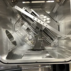
The Materials Characterization Facility (MCF) at Georgia Tech has installed a new inorganic m spectrometry facility. The facility includes two new inductively couple plasma mass spectrometry (ICP-MS) systems: a Thermo iCAP RQ quadrupole ICP-MS for streamlined and high-throughput determinations of elemental concentrations and a Thermo Neoma multicollector ICP-MS with collision cell technology for the precise determinations of isotope ratios within a given sample.
Each instrument can measure elemental variability in both dissolved aqueous samples as well as solids/minerals via laser ablation microsampling from a Teledyne Iridia laser ablation system. Together the system can measure isotopes at precision in elemental systems from Li and U.
Planned applications include: (1) high-resolution measurements of Ca, Sr, Ba, Mg, and B elemental and isotopic variability in seawater and marine and terrestrial carbonates for paleoclimate reconstructions, (2) (U-Th)/Pb dating and Hf isotope measurements to study the origin of critical mineral deposits, with a potential engineering application and the development of novel methods for increasing precision/accuracy and minimizing sample consumption during routine analyses of water quality and environmental contamination.
The MCF welcomes users interested in these and other potential applications of this new facility to their scientific and engineering research to contact David Tavakoli (atavakoli6@gatech.edu).
News Contact
David Tavakoli (atavakoli6@gatech.edu).
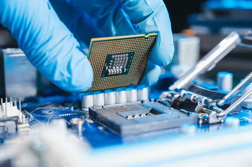
This country’s semiconductor chip shortage is likely to continue well into 2022, and a Georgia Tech expert predicts that the U.S. will need to make major changes to the manufacturing and supply chain of these all-important chips in the coming year to stave off further effects.
That includes making more of these chips here at home.
Madhavan Swaminathan is the John Pippin Chair in Electromagnetics in the School of Electrical and Computer Engineering. He also serves as director of the 3D Systems Packaging Research Center.
As an author of more than 450 technical publications who holds 29 patents, Swaminathan is one of the world’s leading experts on semiconductors and the semiconductor chips necessary for many of the devices we use every day to function.
“Almost any consumer device that is electronic tends to have at least one semiconductor chip in it,” Swaminathan explains. “The more complicated the functions any device performs, the more chips it is likely to have.”
Some of these semiconductor chips process information, some store data, and others provide sensing or communication functions.
In short, they are crucial in devices from video games and smart thermostats to cars and computers.
Our current shortage of these chips began with the Covid-19 pandemic. When consumers started staying at home and car purchases took a downward turn, chip manufacturers tried to shift to make more chips for other goods like smartphones and computers.
But Swaminathan explains that making that kind of switch is not simple. Entire production operations have to be changed. The chips are highly sensitive and can be damaged by static electricity, temperature variations, and even tiny specks of dust. The manufacturing environments must be highly regulated, and changes in the process can add months.
The pandemic highlighted another challenge with the semiconductor chip industry, according to Swaminathan.
“There’s a major shortage of companies making chips,” he says. “If you look worldwide, there are maybe four or five manufacturers making 80-90% of these chips and they are located outside of the United States.”
This creates supply chain hiccups with the raw supplies needed to make these chips as well. Add in the fact that many of these companies only design their chips – they don’t manufacture them directly.
“American consumers use 50% of the world’s chips,” Swaminathan says, which creates a serious challenge when the overwhelming majority of those chips are manufactured in other nations.
In the short term, the costs of the chip shortage is being passed on to the consumer. We see this directly with products like PlayStations and Xboxes that are more and more expensive and harder to purchase when the chips necessary for the consoles to function are in short supply.
Beyond 2022, Swaminathan says we need to work to revitalize the industry domestically.
“We need to bring more manufacturing back to the United States,” he says. “The U.S. government has recognized the importance of this semiconductor chip shortage and is trying to address the issue directly.”
That means investing in new plants to manufacture the chips, but America's journey toward chip self-sufficiency will continue to be a work in progress.
“This is a cycle,” Swaminathan explains. “But this is probably the first time where it has had such a major effect in so many different industries.”
But consumers can take direct action on their own in the coming year. “Reduce the number of times you purchase or upgrade electronic devices like phones and cars,” he says. “Then it becomes just a supply problem, not a demand and supply problem.”
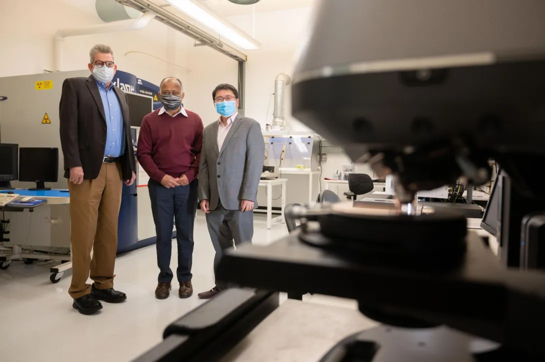
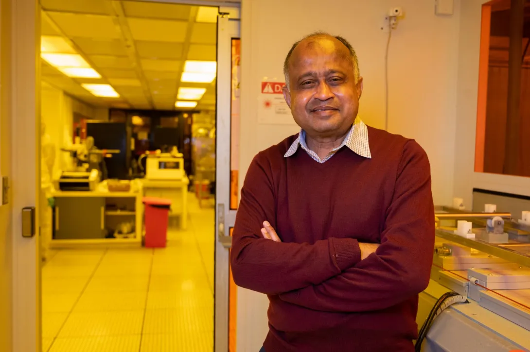
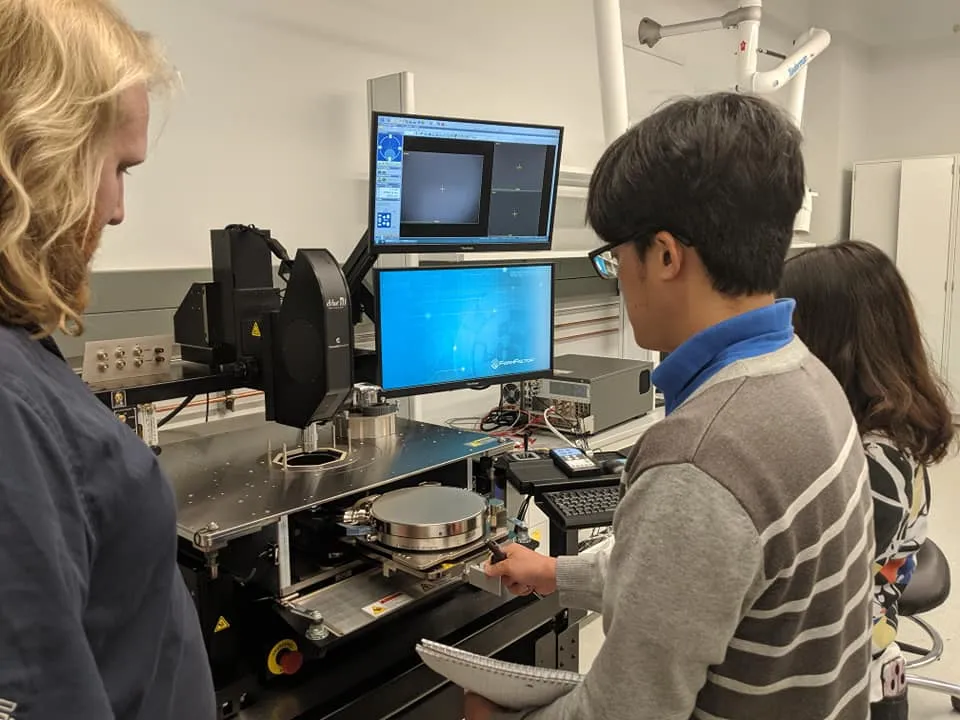
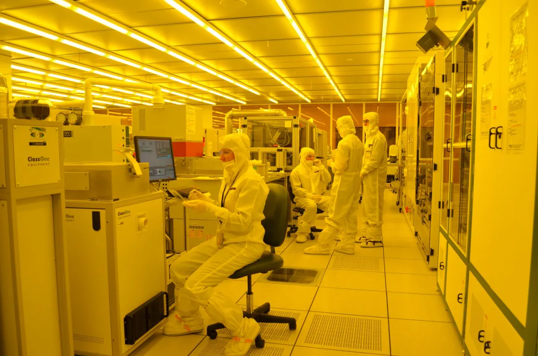
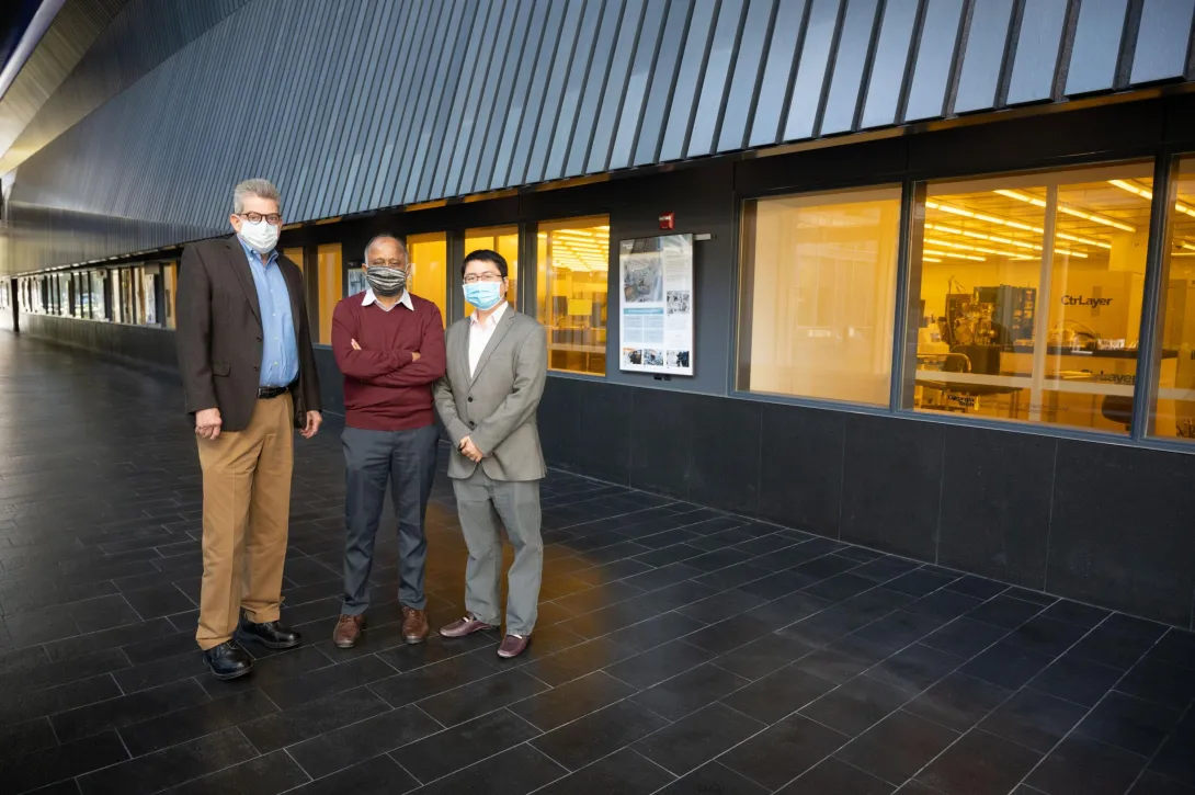
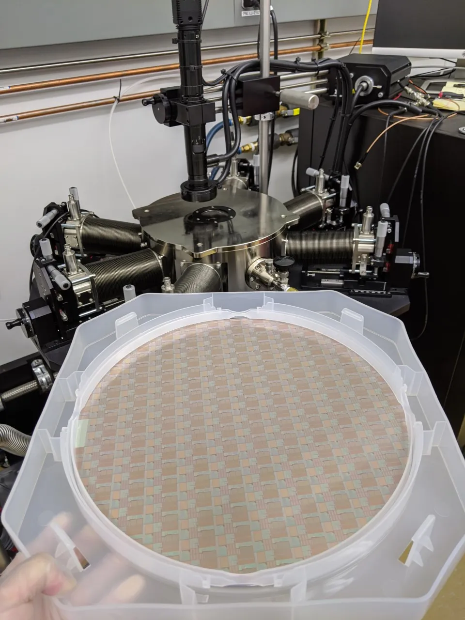
The world’s dependence on semiconductors came into sharp focus in 2021, when automotive manufacturing ground to a halt because of massive computer chip shortages – as Asian suppliers couldn’t keep up with demand for microelectronics – miniaturized electronic circuits and components that drive everything from smartphones to new vehicle components to hypersonics weapons systems.
The culprit was global supply chain disruptions caused by the Covid-19 pandemic. The crisis has highlighted the pressing need for the U.S. to bolster its domestic semiconductor supply chains and industrial capacity, after three decades of decline as a semiconductor producer. The U.S. share of global semiconductor fabrication has dropped to 12% today, compared to 37% in 1990, according to the Semiconductor Industry Association (SIA). In addition, the semiconductor industry today only accounts for 250,000 direct U.S. jobs.
As the country rebuilds its semiconductor infrastructure at home, Georgia Tech serves as a vital partner – to train the microelectronics workforce, drive future microelectronics advances, and provide unique fabrication and packaging facilities for industry, academic and government partners to develop and test new solutions.
“We’re one of the only universities that can support the whole microelectronics stack – from new materials and devices to packaging and systems,” said Madhavan Swaminathan, the John Pippin Chair in Microsystems Packaging in the School of Electrical and Computer Engineering and director of the 3D Systems Packaging Research Center.
News Contact
When cell phones, electric vehicle chargers, or other electronic devices get too hot, performance degrades, and eventually overheating can cause them to shut down or fail. In order to prevent that from happening researchers are working to solve the problem of dissipating heat produced during performance. Heat that is generated in the device during operation has to flow out, ideally with little hinderance to reduce the temperature rise. Often this thermal energy must cross several dissimilar materials during the process and the interface between these materials can cause challenges by impeding heat flow.
A new study from researchers at the Georgia Institute of Technology, Notre Dame, University of California Los Angeles, University of California Irvine, Oak Ridge National Laboratory, and the Naval Research Laboratory observed interfacial phonon modes which only exist at the interface between silicon (Si) and germanium (Ge). This discovery, published in the journal Nature Communications, shows experimentally that decades-old conventional theories for interfacial heat transfer are not complete and the inclusion of these phonon modes are warranted.
“The discovery of interfacial phonon modes suggests that the conventional models of heat transfer at interfaces which only use bulk phonon properties are not accurate,” said the Zhe Cheng, a Ph.D. graduate from Georgia Tech’s George W. Woodruff School of Mechanical Engineering who is now a postdoc at University of Illinois at Urbana-Champaign (UIUC). “There is more space for research at the interfaces. Even though these modes are localized, they can contribute to thermal conductance across interfaces.”
The discovery opens a new pathway for consideration when engineering thermal conductance at interfaces for electronics cooling and other applications where phonons are majority heat carriers at material interfaces.
“These results will lead to great progress in real-world engineering applications for thermal management of power electronics,” said co-author Samuel Graham, a professor in the Woodruff School of Mechanical Engineering at Georgia Tech and new dean of engineering at University of Maryland. “Interfacial phonon modes should exist widely at solid interfaces. The understanding and manipulation of these interface modes will give us the opportunity to enhance thermal conductance across technologically-important interfaces, for example, GaN-SiC, GaN-diamond, β-Ga2O3-SiC, and β-Ga2O3-diamond interfaces.”
Presence of Interfacial Phonon Modes Confirmed in Lab
The researchers observed the interfacial phonon modes experimentally at a high-quality Si-Ge epitaxial interface by using Raman Spectroscopy and high-energy resolution electron energy-loss spectroscopy (EELS). To figure out the role of interfacial phonon modes in heat transfer at interfaces, they used a technique called time-domain thermoreflectance in labs at Georgia Tech and UIUC to determine the temperature-dependent thermal conductance across these interfaces.
They also observed a clean additional peak showing up in Raman Spectroscopy measurements when they measured the sample with Si-Ge interface, which was not observed when they measured a Si wafer and a Ge wafer with the same system. Both the observed interfacial modes and thermal boundary conductance were fully captured by molecular dynamics (MD) simulations and were confined to the interfacial region as predicted by theory.
“This research is the result of great team work with all the collaborators,” said Graham. “Without this team and the unique tools that were available to us, this work would not have been possible.”
Moving forward the researchers plan to continue to pursue the measurement and prediction of interfacial modes, increase the understanding of their contribution to heat transfer, and determine ways to manipulate these phonon modes to increase thermal transport. Breakthroughs in this area could lead to better performance in semiconductors used in satellites, 5G devices, and advanced radar systems, among other devices.
The epitaxial Si-Ge samples used in this research were grown at the U.S. Naval Research Lab. The TEM and EELS measurements were done at University of California, Irvine and Oak Ridge National Labs. The MD simulations were performed by the University of Notre Dame. The XRD study was done at UCLA.
This work is financially supported by U.S. Office of Naval Research under a MURI project. The EELS study at UC Irvine is supported by U.S. Department of Energy.
Citation: https://doi.org/10.1038/s41467-021-27250-3
About Georgia Institute of Technology
The Georgia Institute of Technology, or Georgia Tech, is a top 10 public research university developing leaders who advance technology and improve the human condition. The Institute offers business, computing, design, engineering, liberal arts, and sciences degrees. Its nearly 44,000 students representing 50 states and 149 countries, study at the main campus in Atlanta, at campuses in France and China, and through distance and online learning. As a leading technological university, Georgia Tech is an engine of economic development for Georgia, the Southeast, and the nation, conducting more than $1 billion in research annually for government, industry, and society.
Contact:
Ben Wright
Communications Manager
George W. Woodruff School of Mechanical Engineering
ben.wright@me.gatech.edu