
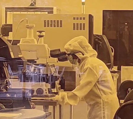
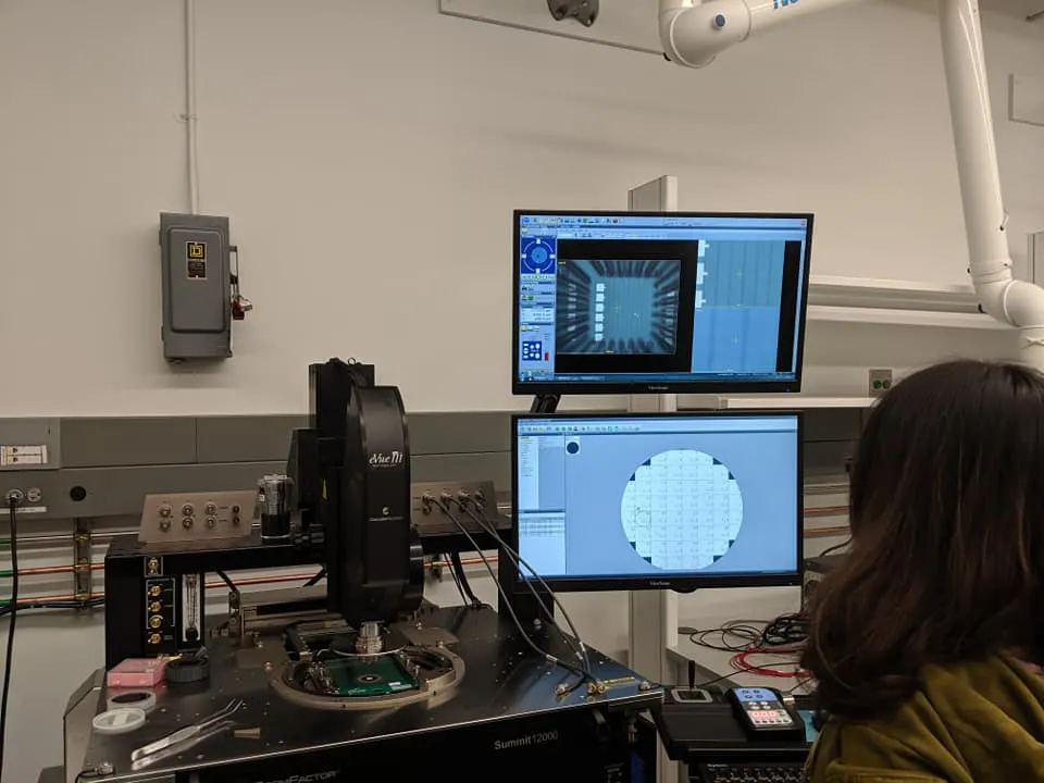
With holiday shopping deadlines looming, consumers cannot escape the impact of the global microelectronic chip shortage. From daily news reports about manufacturers unable to complete orders due to the lack of chips, to “out of stock” messages across websites on popular electronics items, one of the impacts of COVID was to lay bare the massive importance of the microelectronic chip in daily modern life, and how a single-location centered manufacturing nexus can upend the consumer market on a massive scale. The combination of these real-world impacts on supply chains, as well as the need to localize semiconductor and chip manufacturing gave Congress the impetus to pass the “Creating Helpful Incentives to Produce Semiconductors for America Act (CHIPS)”. CHIPS seeks to increase investments and incentives to support U.S. semiconductor manufacturing, research and development, and supply chain security.
The Georgia Institute of Technology was the first university to offer a comprehensive curriculum on microelectronics and microsystems design and packaging and, currently, numerous faculty at Georgia Tech are widely known for their work in semiconductor and microelectronics technologies. In December of 2021 Georgia Tech researchers will again showcase how their pushes the boundaries of microelectronics technologies at the IEEE International Electron Devices Meeting (IEDM).
The School of Electrical and Computer Engineering research teams of Assistant Professor Asif Khan, partnering with Dan Fielder Professor Muhannad Bakir, and Associate Professor Shimeng Yu, partnering with Professor Sung-Kyu Lim and Assistant Professor Shaolan Li, have dominated the 2021 IEDM presentation line-up with a total of 8 accepted papers. With topics ranging from ferroelectric materials for memory, new advances in ALD process, and in-memory computing and 3D reconfigurable architectures, the research presented by these teams is at the cutting-edge of advancing computing power and consumer electronics. In addition to the research presentations, Electrical and Computing Engineering Faculty & Director of the 3D Systems Packaging Research Center at GT will be presenting a short course session on devoted to “Heterogenous Integration Using Chiplets & Advanced Packaging”
Noting the timely nature of these research advancements, Arijit Raychowdhory; Professor and Steve W. Chaddick School Chair in Electrical and Computer Engineering noted, “IEDM is a premier conference in the area of semiconductor devices. Such a strong performance by GT ECE exemplifies the strength of our program, the ingenuity of our students and the innovation driven by our world-class faculty. Sincere congratulations to Professors Khan, Yu Bakir, Lim and Li for their pioneering research in semiconductor logic and memory technologies, that are critical for our nation and our industries.”
Asif Khan is an assistant professor in the School of Electrical and Computer Engineering at the Georgia Tech. He received his Ph.D. in electrical engineering and computer sciences from the University of California, Berkeley in 2015. His work led to the first experimental proof-of-concept demonstration of the negative capacitance effect in ferroelectric oxides. His group at Georgia Tech conceptualizes and fabricates electronic devices that leverage interesting physics and novel phenomena in emerging materials (such as ferroelectrics, antiferroelectrics and strongly correlated systems) to overcome the “fundamental” limits in computation and to address the most pressing challenges in electronics and the semiconductor industry.
Shimeng Yu is currently an associate professor in the School of Electrical and Computer Engineering at the Georgia Tech. He received the B.S. degree in microelectronics from Peking University in 2009, and the M.S. degree and Ph.D. degree in electrical engineering from Stanford University in 2011 and 2013, respectively. From 2013 to 2018, he was an assistant professor at Arizona State University. Prof. Yu’s research interests are the semiconductor devices and integrated circuits for energy-efficient computing systems. His research expertise is on the emerging non-volatile memories for applications such as deep learning accelerator, in-memory computing, 3D integration, and hardware security.
Muhannad S. Bakir is the Dan Fielder Professor in the School of Electrical and Computer Engineering at Georgia Tech. Dr. Bakir and his research group have received more than thirty paper and presentation awards including six from the IEEE Electronic Components and Technology Conference (ECTC), four from the IEEE International Interconnect Technology Conference (IITC), one from the IEEE Custom Integrated Circuits Conference (CICC), and two from the IEEE Transactions on Components Packaging and Manufacturing Technology (TCPMT). Muhannad S. Bakir received the B.E.E. degree from Auburn University, Auburn, AL, in 1999 and the M.S. and Ph.D. degrees in electrical and computer engineering from the Georgia Tech in 2000 and 2003, respectively. His research interests include, heterogeneous microsystem design and integration, including 2.5D and 3D ICs and packaging, electrical and photonic interconnects, and embedded cooling technologies.
Sung Kyu Lim received B.S. (1994), M.S. (1997), and Ph.D. (2000) degrees all from the Computer Science Department at UCLA. During 2000-2001, he was a post-doctoral scholar at UCLA, and a senior engineer at Aplus Design Technologies, Inc. Lim joined the School of Electrical and Computer Engineering at Georgia Institute of Technology an assistant professor. He is currently the director of the GTCAD (Georgia Tech Computer Aided Design) Laboratory and focuses on VLSI and 3D circuit architecture and packaging.
Shaolan Li received his B.Eng. degree with highest honor from the Hong Kong University of Science and Technology (HKUST) in 2012, and his Ph.D. from UT Austin in 2018, all in electrical engineering. Prior joining Georgia Tech as an assistant professor in 2019, he was a post-doctoral fellow in the Department of Electrical and Computer Engineering at UT Austin from 2018-2019. He also held intern positions in Broadcom Ltd. in Sunnyvale, California, and NXP in Tempe, Arizona during 2013-2014. His research interests are broadly in analog, mixed-signal, and RF integrated circuits. His expertise is in high-performance data converters, ultra-low-power low-cost sensor interface, and novel analog mixed-signal architectures for design automation.
The IEEE International Electron Devices Meeting (IEDM) is the world’s preeminent forum for reporting technological breakthroughs in the areas of semiconductor and electronic device technology, design, manufacturing, physics, and modeling. IEDM is the flagship conference for nanometer-scale CMOS transistor technology, advanced memory, displays, sensors, MEMS devices, novel quantum and nano-scale devices and phenomenology, optoelectronics, devices for power and energy harvesting, high-speed devices, as well as process technology and device modeling and simulation. Georgia Tech research teams have a strong track of record in IEDM publications in the recent years, including 8, 4, 9 and 7 papers presented in IEDM 2018, 2019, 2020 and 2021, respectively.
- Christa M. Ernst
News Contact
Christa M. Ernst - Interdisciplinary Research Communications Program Manager
Topics: Materials | Nanotechnology | Robotics
Georgia Institute of Technology| christa.ernst@research.gatech.edu
1. What is your field of expertise and at what point in your life did you first become interested in this area?
I work at the intersection of mechanics, metallurgy, machine learning, and manufacturing. I became interested in engineering as a small child – my grandfather was an engineer, and when I would spend time with my grandparents in the summer, I would go to work with him, and I was fascinated with drawing boards, alligator clips, circuits, and more. In high school, I started interning at the business he had built that primarily developed automation and test equipment for circuit breaker manufacturing (he had passed and my uncle then ran it). I started in the stock room, worked through the machine shop, assembly, and into quality control in my first years there. Then I became an engineering assistant as I went into my undergraduate studies. I had thought that I wanted to be electrical engineer (like my grandfather), but after 6 – 8 months of assisting EE, I realized that my true passion was in mechanical engineering, and I moved over to ME – so that foundation instilled in me that I had a passion for ME, manufacturing, and automation. The metallurgy came years later, when I won a graduate fellowship to work at NASA Glenn while earning my Master’s degree. I worked with metallurgists there who were developing new shape memory alloys, which fascinated me. I resisted materials science and metallurgy for many years, insisting that should be someone else’s job, and I should stick to manufacturing and ME. However, it became evident that you can’t engineer with shape memory alloys or develop their manufacturing unless you deeply understood their metallurgy – that resonated with me when I attended a conference in 2008 while working for a startup company that was commercializing some of the new shape memory alloys the group I’d worked with at NASA had developed. When I returned from that conference, I signed up for my PhD program the next week and dove deep into the intersection of metallurgy, manufacturing, and mechanics. The machine learning came years later, several years into my faculty career. We were working with several companies and the state Office of Economic Development in Colorado (I started my faculty career at Colorado School of Mines) to develop an R&D center and technology incubator to support the growing metals 3D printing industry. When I asked the industry people why they needed a center/consortium at Mines in this area – what were they not getting at other additive manufacturing centers at that time (this was 2014/2015), they said “no one is helping us with our data problems.” So, that became our mission – data informatics innovations in metals additive manufacturing. Here at GT, I’m thrilled by the opportunities, colleagues, and infrastructure available to bring it all together – our big vision for this IMat initiative is to develop R&D test beds and technology incubators for AI materials manufacturing.
2. Why is your theme area important to the development of Georgia Tech’s Materials research strategy?
Largely, our materials research laboratories (nation-wide and globally, not just at Georgia Tech) have been designed and built to support human operators. However, AI cannot independently function in the same way and in the same environments – or, at least, we will never realize its full potential if we make it play by our rules. Re-thinking and designing new materials laboratories that can operate autonomously and semi-autonomously is critical to be at the forefront of future innovations.
3. What are the broader global and social benefits of the research you and your team conduct?
Lowering barriers and times for the discovery and development of new materials and manufacturing – lower costs, faster times to deployment, increased sustainability, and finding better solutions. Also, with AI engines, the ability to distribute manufacturing to local/underserved parts of the globe and our nation – we saw this at the onset of COVID – when our corporate supply chain was unprepared to meet the demand, people were able to contribute respirators, masks, and more using the 3D printers in their garages, libraries, schools, universities, and hospitals and serve their community. However, people in their garages are rarely equipped to qualify/certify/ensure safety of critical parts and widgets on their own – the data infrastructure + AI enables qualification/certification to happen through statistics, and then rapid dissemination of the manufacturing “how to”. One could even imagine a future where the burden of qualification and certification could be shared across everyone participating in the supply chain – that will take a lot of policy and economic reform and rethinking as well, but as we gain confidence in our understanding of statistical models and data management infrastructure and software, it becomes more and more feasible.
4. What are your plans on engaging a wider GT faculty pool with IMat research?
I think the group of involved faculty now spans 7 or 8 schools and 3 colleges, at least – I’ve stopped counting, to be honest – the interest and support of colleagues here at GT is tremendous. On our larger proposals, there are anywhere from 20 – 30 faculty involved – I think this next one we may exceed 40. I welcome anyone who has ideas for how they can contribute or wants to learn more about the vision for AI materials + manufacturing test beds to email me anytime, and we’ll setup a time to meet and discuss. I also intend to hold some workshops and conferences – we received funding to start a consortium that will hold quarterly meetings for any interested business or faculty, and newsletters will also be sent, starting in 2022.
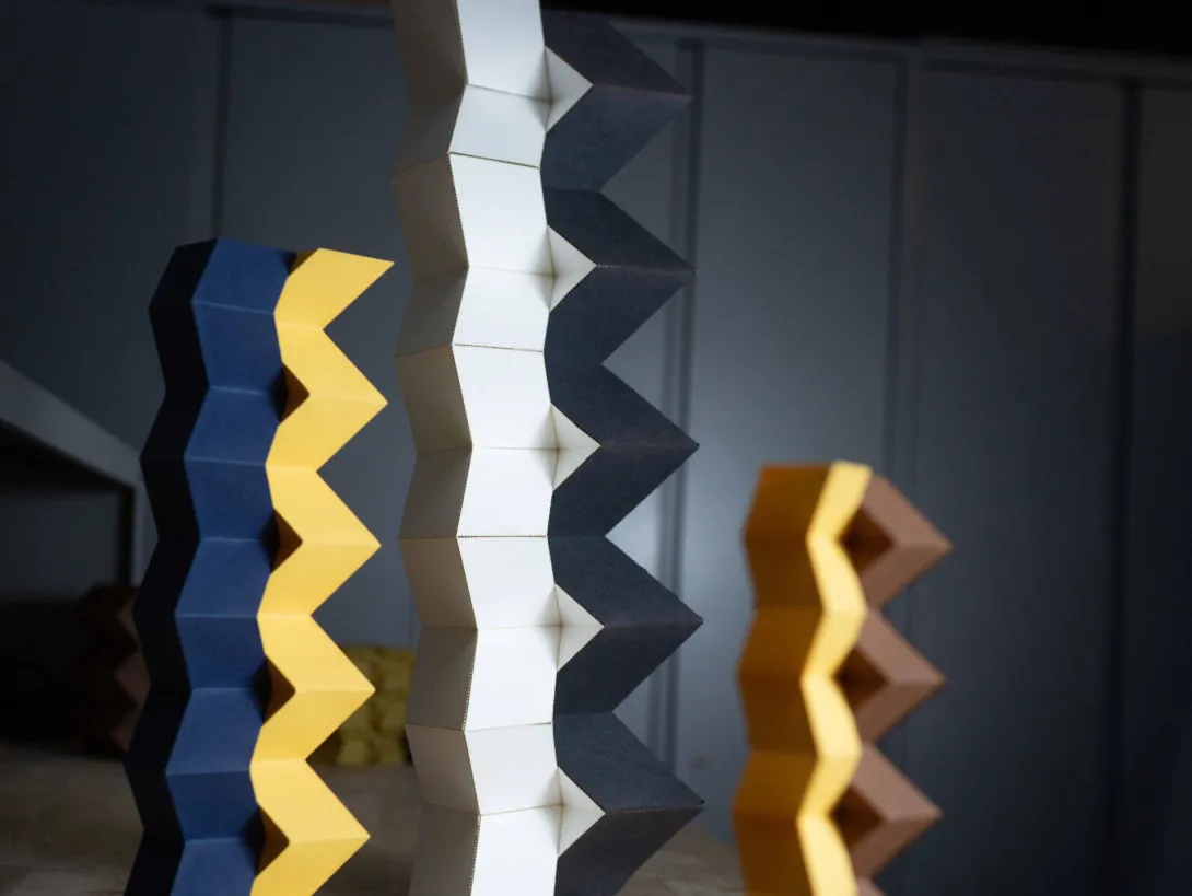
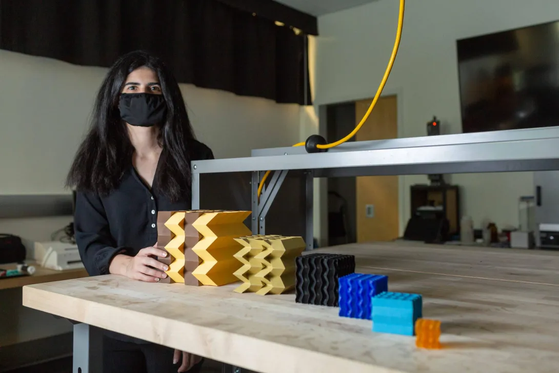
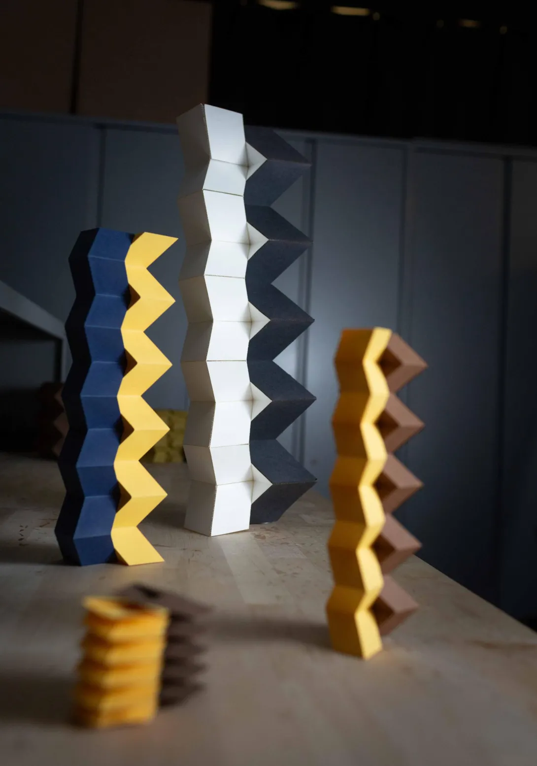
The simplicity and elegance of origami, an ancient Japanese art form, has motivated researchers to explore its application in the world of materials.
New research from an interdisciplinary team, including Northwestern University’s Horacio Espinosa and Sridhar Krishnaswamy and the Georgia Institute of Technology’s Glaucio Paulino, aims to advance the creation and understanding of such folded structures for applications ranging from soft robotics to medical devices to energy harvesters.
Inspired by origami, mechanical metamaterials — artificial structures with mechanical properties defined by their structure rather than their composition — have gained considerable attention because of their potential to yield deployable and highly tunable structures and materials.
What wasn’t known was which structures integrate shape recoverability, pronounced directional mechanical properties, and reversible auxeticity — meaning their lateral dimensions can increase and then decrease when progressively squeezed. Though some 3D origami structures have been produced through additive manufacturing, achieving the folding properties displayed in ideal paper origami remained a challenge.
Using nanoscale effects for an origami design, the team of researchers from Northwestern’s McCormick School of Engineering and Georgia Tech's School of Civil and Environmental Engineering sought to answer that question. They produced small, 3D, origami-built metamaterials, successfully retaining the best properties without resorting to artifacts to enable folding.
“The created structures constitute the smallest fabricated origami architected metamaterials exhibiting an unprecedented combination of mechanical properties,” said Espinosa, the James and Nancy J. Farley Professor of Manufacturing and Entrepreneurship and professor of mechanical engineering and (by courtesy) biomedical engineering and civil and environmental engineering.
“Our work demonstrated that rational design of metamaterials, with a large degree of shape recoverability and direction-dependent stiffness and deformation, is possible using origami designs, and that origami foldability enables a state where the material initially expands and subsequently contracts laterally (reversible auxeticity),” added Espinosa, who serves as director of Northwestern’s theoretical and applied mechanics graduate program. “Such properties promise to influence a number of applications across a wide range of fields encompassing the nano-, micro-, and macro-scales, leveraging the intrinsic scalability of origami assemblies.”
“Guided by geometry, the scaling and miniaturization of the origami metamaterial are exciting in itself and by the unprecedented multifunctionality that it naturally enables,” said Paulino, the Raymond Allen Jones Chair in Georgia Tech’s School of Civil and Environmental Engineering.
“Only an interdisciplinary effort combining origami design, 3D laser printing with nanoscale resolution, and in situ electron microscopy mechanical testing could reveal the unprecedented combination of properties our work demonstrated and their potential impact on future applications,” added Paulino, who contributed to establishing the National Science Foundation Emerging Frontiers in Research and Innovation program named ODISSEI (Origami Design for Integration of Self-assembling Systems for Engineering Innovation).
“Just like nature has architected a wide range of structures using just a few material systems, origami allows us to engineer resilient structural components with distinct physical properties along different directions,” said Krishnaswamy, professor of mechanical engineering.
“We can envision origami-based soft microrobots that are stiff along some directions to carry payloads while maintaining other degrees of flexibility for motion. Origami-metamaterials that exploit reversible auxeticity and large deformation can lead to multifunctional applications ranging from deployable microsurgical instruments and medical devices to energy steering and harvesting,” added Krishnaswamy, the director of Northwestern’s Center for Smart Structures and Materials.
The study presents new avenues to be explored long term, Espinosa said.
“There are a number of possibilities,” he said. “One is the fabrication of origami structures with ceramic and metallic materials, while preserving nanoscale dimensions, to exploit size effects in the mechanical response of the structures leading to superior energy dissipation per unit volume and mass. Another is the use of piezoelectric polymers, which can result in energy harvesters that can drive sensing modalities or power microsurgical tools.”
The research, “Folding at the Microscale: Enabling Multifunctional 3D Origami-Architected Metamaterials” was published in the journal Small on July 27. Along with Espinosa, Krishnaswamy, and Paulino, coauthors include Northwestern’s Nicolas A. Alderete, Zhaowen Lin, and Heming Wei, and Larissa S. Novelino from Georgia Tech.
The research was supported by the Army Research Office (award W911NF1220022), a Multi-University Research Initiative through the Air Force Office of Scientific Research (AFOSR-FA9550-15-1-0009), the Office of Naval Research (grants N00014-15-1-2935 and N00014-16-1-3021), and the National Science Foundation (grant No. 1538830). Nicolas Alderete received a fellowship from the Argentinian Roberto Rocca Education Program and Larisa Novelino from the Brazilian National Council for Scientific and Technological Development (project 235104/2014-0).
Writer: Brian Sandalow, Northwestern University
News Contact
John Toon
Research News
(404) 894-6986
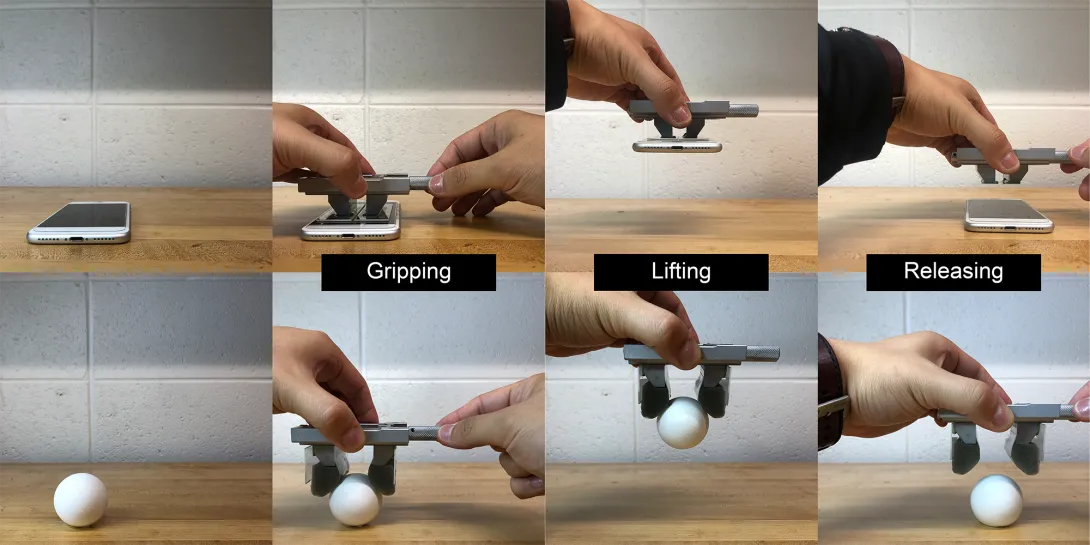
Why did the gecko climb the skyscraper? Because it could; its toes stick to about anything. Engineers can already emulate the secrets of gecko stickiness to make strips of rubbery materials that can pick up and release objects, but simple mass production for everyday use has been out of reach until now.
Researchers at the Georgia Institute of Technology have developed, in a new study, a method of making gecko-inspired adhesive materials that is much more cost-effective than current methods. It could enable mass production and the spread of the versatile gripping strips to manufacturing and homes.
Polymers with “gecko adhesion” surfaces could be used to make extremely versatile grippers to pick up very different objects even on the same assembly line. They could make picture hanging easy by adhering to both the picture and the wall at the same time. Vacuum cleaner robots with gecko adhesion could someday scoot up tall buildings to clean facades.
“With the exception of things like Teflon, it will adhere to anything. This is a clear advantage in manufacturing because we don’t have to prepare the gripper for specific surfaces we want to lift. Gecko-inspired adhesives can lift flat objects like boxes then turn around and lift curved objects like eggs and vegetables,” said Michael Varenberg, the study’s principal investigator and an assistant professor in Georgia Tech’s George W. Woodruff School of Mechanical Engineering.
Current grippers on assembly lines, such as clamps, magnets, and suction cups, can each lift limited ranges of objects. Grippers based on gecko-inspired surfaces, which are dry and contain no glue or goo, could replace many grippers or just fill in capability gaps left by other gripping mechanisms.
Drawing out razors
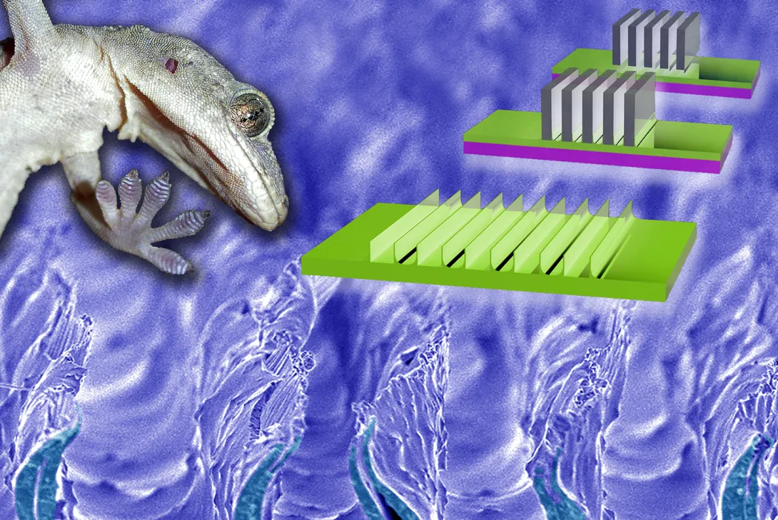
The adhesion comes from protrusions a few hundred microns in size that often look like sections of short, floppy walls running parallel to each other across the material’s surface. How they work by mimicking geckos’ feet is explained below.
Up to now, molding has produced these mesoscale walls by pouring ingredients onto a template, letting the mixture react and set to a flexible polymer then removing it from the mold. But the method is inconvenient.
“Molding techniques are expensive and time-consuming processes. And there are issues with getting the gecko-like material to release from the template, which can disturb the quality of the attachment surface,” Varenberg said.
The researchers’ new method formed those walls by pouring ingredients onto a smooth surface instead of a mold, letting the polymer partially set then dipping rows of laboratory razor blades into it. The material set a little more around the blades, which were then drawn out, leaving behind micron-scale indentations surrounded by the desired walls.
Varenberg and first author Jae-Kang Kim published details of their new method in the journal ACS Applied Materials & Interfaces on April 6, 2020.
Forget about perfection
Though the new method is easier than molding, developing it took a year of dipping, drawing, and readjusting while surveying finicky details under an electron microscope.
“There are many parameters to control: Viscosity and temperature of the liquid; timing, speed, and distance of withdrawing the blades. We needed enough plasticity of the setting polymer to the blades to stretch the walls up, and not so much rigidity that would lead the walls to rip up,” Varenberg said.
Gecko-inspired surfaces have a fine topography on a micron-scale and sometimes even on a nanoscale, and surfaces made via molding are usually the most precise. But such perfection is unnecessary; the materials made with the new method did the job well and were also markedly robust.
“Many researchers demonstrating gecko adhesion have to do it in a cleanroom in clean gear. Our system just plain works in normal settings. It is robust and simple, and I think it has good potential for use in industry and homes,” said Varenberg, who studies surfaces in nature to mimic their advantageous qualities in human-made materials.
[Ready for graduate school with social distancing? Here's how to apply to Georgia Tech.]
Gecko foot fluff
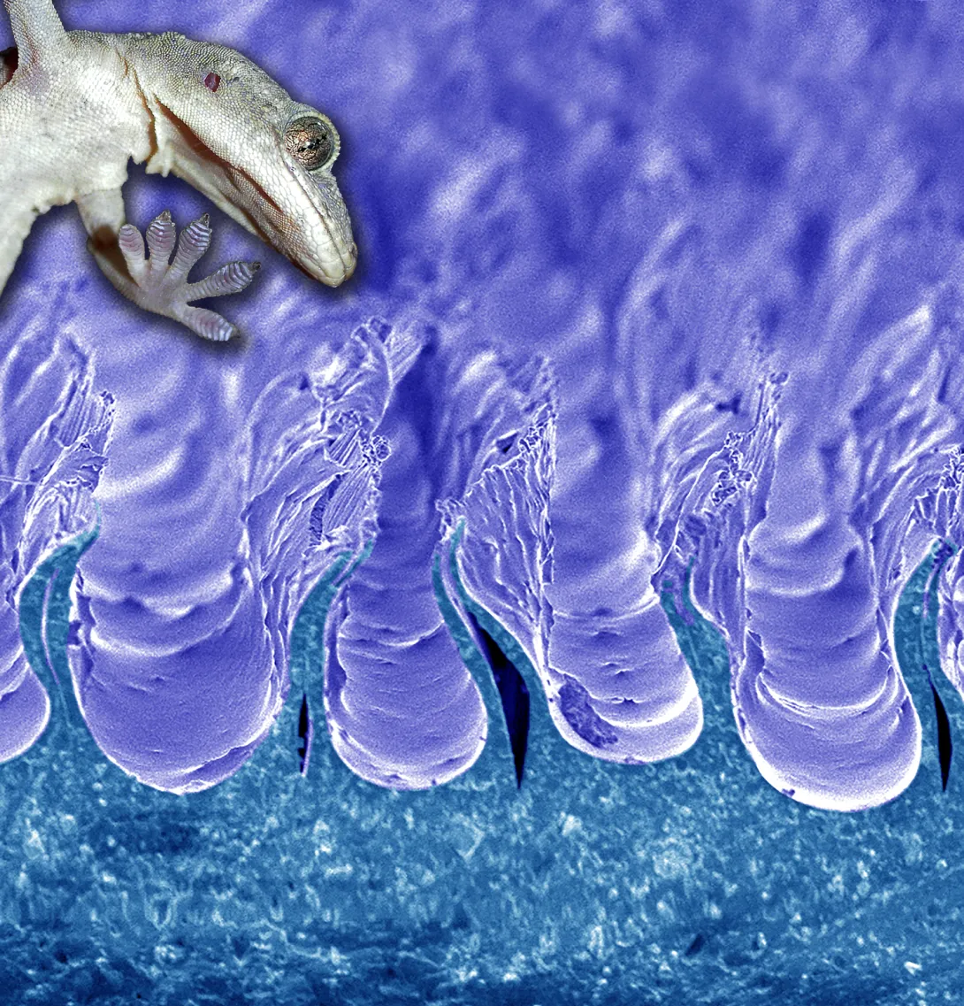
Behold the gecko’s foot. It has ridges on its toes, and this has led some in the past to think their feet stick by suction or some kind of clutching by the skin.
But electron microscopes reveal a deeper structure – spatula-shaped bristly fibrils protrude a few dozen microns long off those ridges. The fibrils make such thorough contact with surfaces down to the nanoscale that weak attractions between atoms on both sides appear to add up enormously to create overall strong adhesion.
In place of fluff, engineers have developed rows of shapes covering materials that produce the effect. A common shape makes a material’s surface look like a field of mushrooms that are a few hundred microns in size; another is rows of short walls like those in this study.
“The mushroom patterns touch a surface, and they are attached straightaway, but detaching requires applying forces that can be disadvantageous. The wall-shaped projections require minor shear force like a tug or a gentle grab to generate adherence, but that is easy, and letting go of the object is uncomplicated, too,” Varenberg said.
Varenberg’s research team used the drawing method to make walls with U-shaped spaces in between them and walls with V-shaped spaces in between. They worked with polyvinylsiloxane (PVS) and polyurethane (PU). The V-shape made in PVS worked best, but polyurethane is the better material for industry, so Vanenberg’s group will now work toward achieving the V-shape gecko gripping pattern in PU for the best possible combination.
Also read: Lung-heart super sensor on a chip tinier than a ladybug
Here's how to subscribe to our free science and technology email newsletter
Writer & Media Representative: Ben Brumfield (404-272-2780), email: ben.brumfield@comm.gatech.edu
Georgia Institute of Technology
Georgia Tech Arts is still seeking projects for the 2021 ACCelerate: ACC Smithsonian
Creativity and Innovation Festival in Washington, DC. All Georgia Tech students, faculty, and staff are invited to apply by May 1, 2020.
Even if you do not have a finished project exploring the intersection of science,
engineering, art, design, and technology, we encourage you to speak with Es
Famojure at esther.famojure@arts.gatech.edu about your concepts.
Learn about Georgia Tech's 2019 participants for some inspiration.
The festival brings together all institutions included in the Atlantic Coast Conference to
celebrate creativity and innovation with a specific focus on science, engineering, arts, and
design. It will be held April 9 -11, 2021 at the Smithsonian National Museum of American
History.
Submit your project for consideration by May 1, 2020 to be considered.
News Contact
Es Famojure
esther.famojure@arts.gatech.edu